3D-IC integration prospects improving, say IEDM researchers
It looks like the performance impact of building systems using 3D-IC integration techniques (Guide) such as thinned wafers and through-silicon vias will be limited, according to two presentations at IEDM this week.
A paper presented by T Lo of the process integration team at TSMC looked at the performance impact of thinning and stacking wafers, and of running TSVs through active areas, for both poly gate and HKMG processes.
An analysis of the performance of nMOS and pMOS devices in both poly and HKMG showed “little to no degradation of performance” due to thinning or stacking, according to Lo.
The analysis also looked at three effects from the mechanical stress induced by the mismatch in thermal expansion coefficients between the silicon lattice and the TSV material. The first was the change in IDsat caused by the TSV, which was smaller for both n and pFETs on HKMG processes than on poly gate processes.
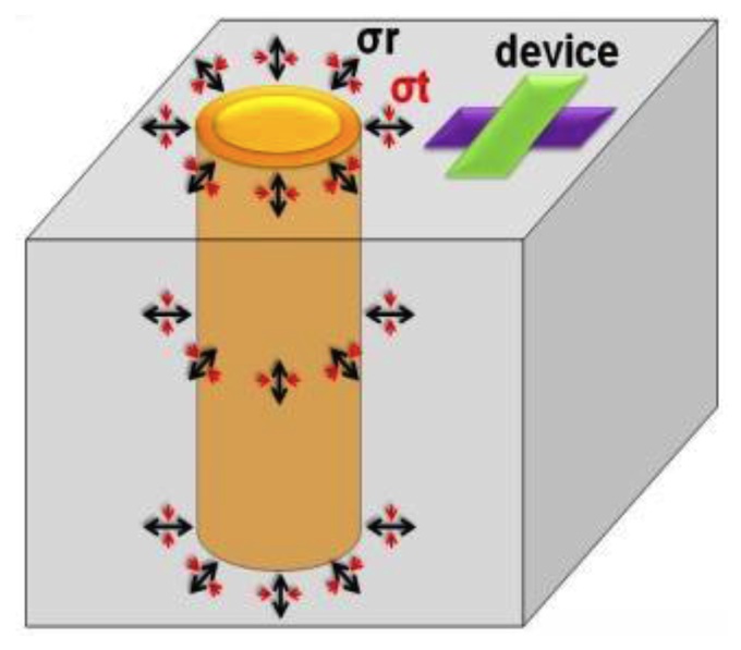
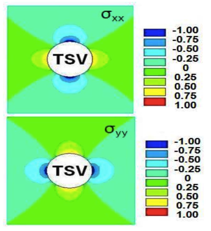
One issue that might be of practical importance in design is the different stresses induced in transistors, depending whether their (source, gate, drain) axis was aligned radially to the TSV, or tangentially. Lo said that the combination of radial tension and tangential compression caused by the TSV created a non-symmetrical stress distribution in the silicon around it that affects carrier mobility and therefore IDsat.
Figure 1 Combining radial and tangential forces creates non-uniform stresses around the TSV (Source: TSMC)
Figure 2 The impact on the transistor varies, depending whether it is aligned radially or tangentially to the TSV (Source: TSMC)
An analysis of the TSV’s performance as a conductor showed good results, with tests run on a daisy chain of TSVs showing a resistance per TSV of just 47mΩ at low frequencies, rising slightly with frequency, while inductance remained flat and capacitance fell. Lo did say, though, that TSMC had had trouble extracting values for the TSV, giving the impression that a proper model had yet to be developed.
Summing up, she added that the TSV’s measured electrical characteristics matched simulation, and that therefore TSMC had a stable process. She wouldn’t, however, specify the diameter of the TSVs used in the tests, or define a keep-out area beyond which users could be confident that their devices would be unaffected by TSV issues.
Inter-die latency in 3D integration schemes may also be less of a problem than expected, at least at advanced process nodes. Asked about the issue during the question and answer session following an earlier paper in the same session focusing on the advantages of embedded DRAM in mainframe processor chips, Subramaniam Iyer, of the Semiconductor Research and Development Center at IBM, said that “when you stack die, you always take a latency hit”, because you have to latch signals at either end of the interconnect. However, as the interconnect becomes smaller and smaller [presumably with more sophisticated stacking schemes], the latency becomes smaller and smaller so “in future the speed of [single chip integration compared with stacking] could be the same.”

