May 29, 2013
How to design with finFETs, including the impact on standard cells, IP, SRAM; the effects of fin quantization; extraction and parasitics; AMS issues and more.
May 2, 2013
A look at some of the design and physical verification challenges of working with finFET and FD-SOI devices, including their impact on layout, DRC and LVS.
April 22, 2013
The arrival of the 20nm and finFET-based 14nm and 16nm processes bring with them challenges for custom IC design. These are the five key areas and a methodology that can address them.
December 4, 2012
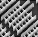
finFETs are vital to the next generation of CMOS processes from Intel, TSMC and others. How will process issues including bulk vs SOI substrates, density limitations, thickness control, and planar device integration affect their practical implementation?
March 28, 2012
It may be necessary to move to three-dimensional 'FinFET' transistors for future process nodes, but what impact will this have on circuit design?
August 23, 2011
Intel says ‘trigate’—finFET to others—but depleted silicon-on-insulator also has its post 22nm supporters. Chris Edwards reports on the debate at 2011’s Semicon West.