How to design with finFETs
How to design with finFETs, including the impact on standard cells, IP, SRAM; the effects of fin quantization; extraction and parasitics; AMS issues and more.
The finFET (Guide) is being promoted as the basic device for future IC processes, now that the scaling of planar transistors is no longer bringing the performance and power-consumption advantages to which the industry has become accustomed. What are the advantages and challenges of finFETs, and what impact will they have on design? This piece on how to design with finFETs, drawn from a Synopsys webinar, explores the issues.
The device
In planar transistors, a ‘gate’ electrode above a conducting channel, separated from it by an insulating layer, creates an electric field that controls the flow of charge carriers between source and drain through that channel. As the minimum dimensions of IC processes have shrunk, unwanted leakage currents have grown, particularly between source and drain. To counter this leakage the channel has been increasingly heavily doped, which has reduced carrier mobility and therefore device performance. To overcome this issue in turn, the channel has been subjected to mechanical strain, usually by applying a material with a slight lattice mismatch, to repair carrier mobility.
The result has been an increasingly complex planar device, the performance advantages of which have narrowed with each successive process node. Planar devices are also increasingly subject to issues such as performance variability due to statistical variations in dopant concentrations.
Experiments in the late 1990s showed that building a gate below, as well as above, the channel of a planar transistor, and reducing the channel’s thickness so the gates had better control over it, could dramatically reduce leakage. In one experiment, halving the thickness of the channel from 20nm to 10nm in a double-gate planar transistor reduced its leakage 8000-fold.
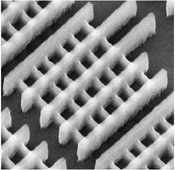
Turning the double-gate device through 90 degrees, so that the channel is built in a fin orthogonal to the surface of the silicon with a gate electrode deposited over it, creates a single gate formation that means it is possible to control the channel from both sides. Channel-thickness experiments show that the thinner the fin, the lower the leakage, while making the fin taller (within the limits of reliable etching) improves its drive strength. The distance between fins (their pitch) determines the area each device will take in a layout, although there’s a trade-off between making the fins closer together, which increases density but limits the tilt angle available to implant the source and drain, and performance.
Figure 1An SEM of Intel’s high-speed, low-power finFET variant on its 22nm process (Source: Intel)
FinFET advantages
Intel has taken the lead in implementing finFET (or what it calls TriGate devices) in its manufacturing processes. In a comparison of Intel’s TriGate process with its 32nm planar process, Intel found an order-of-magnitude improvement in leakage performance at the same operating voltage. The finFET can also be run at a lower operating voltage for a given leakage current, halving its dynamic power consumption (which is proportional to CV2f) for a 0.7 scaling in VDD.
Some of these advantages become more significant as the operating voltage is reduced. At 1V, the finFET is 18% faster than the equivalent planar device, but at 0.7V, the advantage is 37%. This is because the finFET’s sub-threshold swing (the amount that the threshold voltage has to be changed to halve its leakage) is lower than in a planar device, so the device can be operated at lower threshold voltages for the same leakage. This, in turn, means that the difference between the gate and threshold voltage at very low operating voltages is much greater, exaggerating the performance advantage of very low-voltage finFETs.
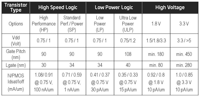
Intel has taken this work forward in its 22nm process, which adapts a basic finFET for high-performance, low-power or high-voltage operation in SoCs.
Figure 2 Basic parameters of four variants of Intel’s latest, 22nm finFET process (Source Intel IEDM 2012)
Along with low leakage, other advantages of the finFET include lower threshold-voltage variability, because the channel is so well controlled that it doesn’t need heavy doping and is therefore less susceptible to random dopant fluctuations.
FinFETs also offer well-matched IDsat performances for N- and P-type devices, which may simplify some aspects of design, and a reasonable ratio between On and Off currents.
The fact that the effective width of the finFET is defined by twice its height plus its thickness means that it has a significant advantage in effective transistor width (and therefore in terms of IDsat per linear distance) over planar devices for logic designs. The advantage is greater for SRAM layouts, given their dense nature.
These issues can be explored using technology CAD tools, which can model and simulate new devices.
FinFET design issues and tools impact
The finFET is not without its issues, some of which will have an impact on the way that design is done and hence the tool support that will be necessary to work with them.
Among these issues are:
- • More complex Spice models and parasitic RC extraction requirements
- • Quantized transistor widths
- • Increased layout dependency issues
SoC designers, such as Achronix, should find that a lot of these issues are transparent to them, since they will be handled at the process, device, or standard-cell level, or within tools such as place and route. Standard cell and IP designers won’t face huge changes in approach, although design rules may become restrictive. Memory designers may face greater challenges, and custom design and analog IP specialists will have to spend more time managing transistor parasitics.
Although the overall design flow hasn’t changed, it is unlikely that a design laid out for a planar process can be mapped directly to a finFET process. Layouts will probably have to be done again, from scratch.
Spice models and parasitic RC extraction
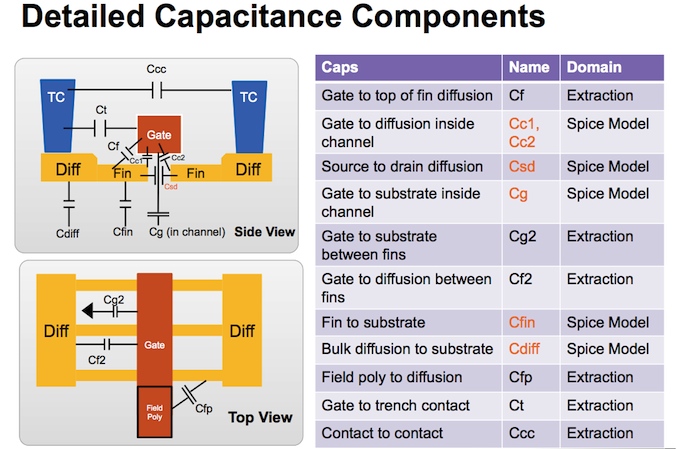
The three-dimensional complexity of finFETs, especially the number of layers between the device and Metal 1, makes modeling their internal parasitics more complex than modeling planar devices.
The manufacture of finFETs also brings modeling issues. In a planar device, the source and drain are self-aligned with the gate and often intrude slightly under it. In finFET manufacture, there’s a spacer between the gate and the source and drain, which are usually raised and have a strain on them, thanks to a SiGe layer that creates a lattice mismatch. This means there are much more complex parasitics to be accounted for within a finFET Spice model.
The BSIM Group of the UC Berkeley Device Group has developed a compact model, known as BSIM-CMG (for common multi-gate), which accounts for these 3D effects and the multi-gate nature of finFET devices. It adds new parameters such as the number of fins, poly direction and others to the planar BSIM model. Parameters such as W are removed.
Complex parasitics
The fact that fins are 3D structures that rise above the substrate means that they are more strongly affected by their immediate environment than planar devices. This means coordinating the BSIM-CMG model of the device, which expresses factors that don’t vary with context, and a model, expressed in the extracted netlist, of the interaction between the device and its surroundings.
Figure 3 What goes where: how layout-dependent and layout-independent parasitics are divided between Spice model and extracted netlist (Source: Synopsys)
It’s here that a designer’s layout experience can make a difference in saving on parasitics when given various choices with which to realize a design.
Quantization
Because the point of a finFET is to achieve better electrostatic control of the channel, and because of etch uniformity requirements, the thickness and the height of the fin cannot be changed arbitrarily, as in a planar device. So finFET transistor widths are quantized, with greater drive currents being achieved by ganging together several discrete fins, with the same source, drain and gate. This quantization may cause flexibility issues, especially in analog design, although designers should be able to adapt to the new constraint.
Increased layout dependencies
Layout details have an impact on the stress profile of the finFET, and hence on its carrier mobility. These details have different effects depending upon whether the fins are situated between two other fins; are at the end of a row of fins; or are isolated.
SiGe depositions in the source and drain areas cut the parasitic resistivity of the source and drain, and create strain that enhances carrier mobility. Fins that are not supported in all directions tend to ‘relax’ with the strain induced by the SiGe lattice mismatch collapsing, reducing the mobility enhancement and leading to a potential significant deterioration of drive current.
Modeling a multi-fin device therefore means accounting for different device behaviours that depend on the number of fins and the ratio of ‘end’ to ‘middle’ fins – or using extra layout area to add ‘dummy’ fins that sustain the stress in these ‘lonely’ finFETs.
Isolation, body bias and thermal considerations
The isolation of the finFET’s channel above the substrate means that it is not reasonable to use body biasing to adjust device performance. The physical isolation of the finFET may also lead to self-heating issues, especially when used in circuits with a heavy duty cycle such as clocks. Finally, the isolated nature of the fins make a finFET a poor ESD device.
Manufacturing
Manufacturing high aspect-ratio fins and depositing good-quality insulating and gate layers over them is a challenge, especially in terms of lithography, where either double-patterning techniques or directional etch technology have to be used to shape the fins. Increased process complexity also means increased cost.
The SRAM cell as an example
Many of these issues are brought together in the design of SRAM cells in finFET processes.
The good news is that finFET SRAMs have higher performance and lower leakage than planar equivalents, and can operate at lower operating voltages. The devices offer good static noise margins at these low voltages, because dopant-based variability is low, and it’s possible to achieve good noise to signal ratios. Read and Write margins are smaller, and their distribution narrower, because of the lower operating voltage.
The challenges for SRAM designers working with finFET processes include the fact that the basic device’s beta ratio is quantized, and therefore cannot be fine tuned. The narrower static noise margins resulting from quantized beta and lower VDD operation pose challenges for both the Read and Write margins, so designers need to add assist circuitry to ensure reliable operation. Body biasing doesn’t work, so new ways to control leakage must be developed. And self heating may be a problem, since fins are less efficiently cooled.
As processes become denser, the channel area will decrease and threshold voltage variability will increase, challenging SRAM designers. The resistance and capacitance of the source and drain regions also present a hurdle to good finFET SRAM performance. And those who are trying to develop such IP need mature device models that capture finFET effects associated with new surface orientation, surface scattering, ballistic transport, corner effects, and more.
Conclusions
The good news about finFETs is that they mitigate many of the short-channel effects that have meant that moving to the next planar process generation has begun to offer diminishing returns. FinFETs also have attractive qualities, such as the ability to tune their performance for energy efficiency or performance, which means they can be used as the basis of flexible SoC processes.
The trade-off is that designers will have to learn to work with the new BSIM-CMG models, and extracted netlists that pile environmental parasitics on top of the complex internal parasitics of the devices themselves. Analog and custom circuit designers will also have to learn to live in a world in which key parameters are now parameterised.
For many designers, the shift to finFET-based processes will be hidden in the many levels of abstraction used by the EDA industry to make complex designs tractable. But there will still be plenty of change to accommodate as manufacturing processes mature and design experience grows.


