Three ways to 3D feature at IEDM
The use of 3D integration to improve IC design will feature at the International Electron Device Meeting (IEDM) in December, which returns to a physical format this year. Three highlighted papers at the conference show the different approaches to the use of the vertical dimension to cut energy use and improve density.
A number of teams have proposed using monolithic 3D integration as a way of slashing the energy consumption of machine-learning implementation. The reduction in wire length for memory transactions could make a huge difference in applications like this where the memory usage is a major component of the overall power budget. Examples include the N3XT architecture proposed by Professor Philip Wong of Stanford and chief scientist at TSMC, which stacks resistive memory (ReRAM) arrays on top of silicon CMOS logic.
Researchers at Tsinghua University and the Chinese Academy of Sciences have taken a slightly different approach with a design aimed at one-shot learning applications by making the ReRAM array a ternary content-address memory (TCAM). According to the team’s experiments energy consumption is 160 times lower than a software implementation running on a GPU.
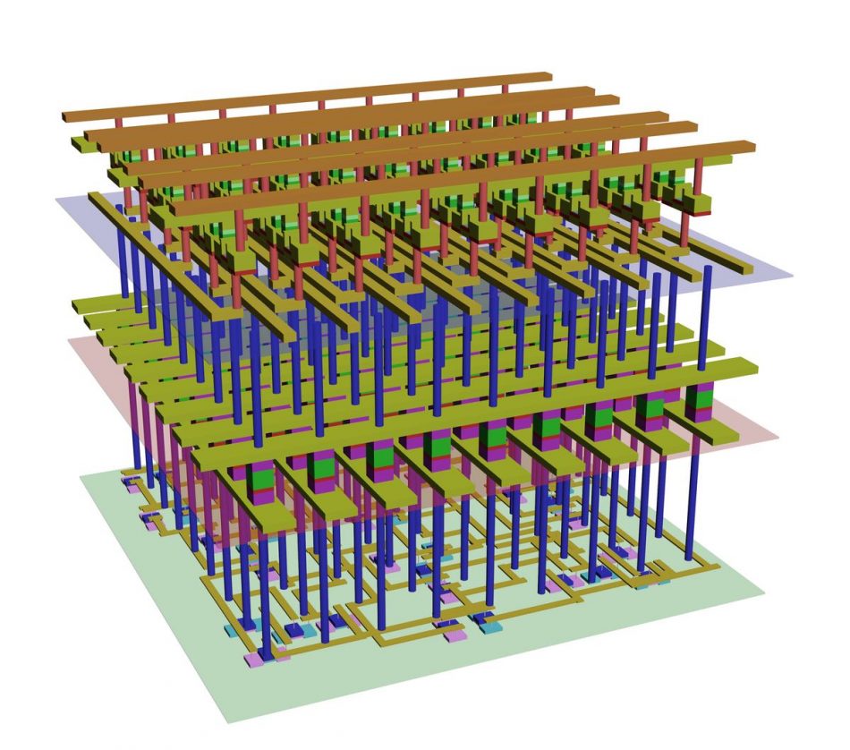
Image 3D projection of the TCAM and logic array
As a major proponent of another form of monolithic 3D integration that could be used in mainstream production, Imec has continued to work on its buried power rail concept. This will boost effective interconnect density by moving many of the power rails that today need to be allocated to lower metal layers into the silicon substrate.
One question is what those power rails should be made of: there are serious issues with some of the options because of the incompatibility that some high-conductivity metals have with transistor-forming processes. Working with nearby deposition specialist ASM International, a team from Imec has used experiments on 1nm, 2nm, and 3nm-class processes to determine that they may need different metal combinations. For the 3nm process node, a tungsten power rail looks to be best for line and contact resistance whereas for smaller geometries, molybdenum looks to be a better choice for the power rail, with ruthenium for the vias.
Vertical transistor structures are now the norm in flash memory and the arrival of the finFET began an evolution of logic transistors into forms that could exploit the third dimension for both density and short-channel control improvements. As processes begin to transition to nanosheets at the 3nm and 2nm nodes, fabs are using stacking techniques to improve current delivery. The next step after that would be turn the transistor through 90 degrees so that the channels are arranged vertically. In principle, this overcomes one key problem with further scaling: the IRDS projections are for gate-length scaling to stop at around 12nm using silicon-based materials. A vertical structure makes it possible to keep a longer gate and still scale interconnect and gate pitch as well as spacer size.
In an experiment into making vertical nanosheet transistors, IBM and Samsung used a 45nm gate pitch and found they could make big reductions in capacitance compared to a lateral reference design. To test the concept the team made functional ring oscillators and obtained a 50 per cent cut in capacitance.
The overall theme for the 67th annual IEDM, to be held December 11–15, 2021 at the Hilton San Francisco Union Square hotel, “Devices for a New Era of Electronics: From 2D Materials to 3D Architectures”, as another element of the conference will be the growing interest in 2D materials such as molybdenum disulphide as well the novel architectures that are being applied to power semiconductors.