Chiplet design raises big questions
An online conference organized by the trade group MEPTEC last week (July 13-14, 2021) provided insights into how SoC design may evolve into system-in-package based on the use of chiplets. It is a change that has many more subtleties than simply trying to divide an SoC into components that straddle multiple die.
A major factor in how chiplet-based designs will evolve lies in the markets that will adopt them. Using projections put together in 2019 by IHS Markit, Synopsys strategy and systems architect Ming Zhang said, “The primary applications are driven by demand for bigger chips for servers and AI, with a little bit of telecom.”
It is not just a question of size but how the silicon area is used. ASE fellow Bill Chen said “We are going into a time of application-specific computing”. That means much greater use of accelerators rather than simply spawning general-purpose compute cores. However, trying to rework SoCs for a large number of different applications quickly becomes financially prohibitive. Putting accelerators into chiplets alongside more generic central processing units (CPUs) together with network I/O and memory controllers provides a way to align the two needs.
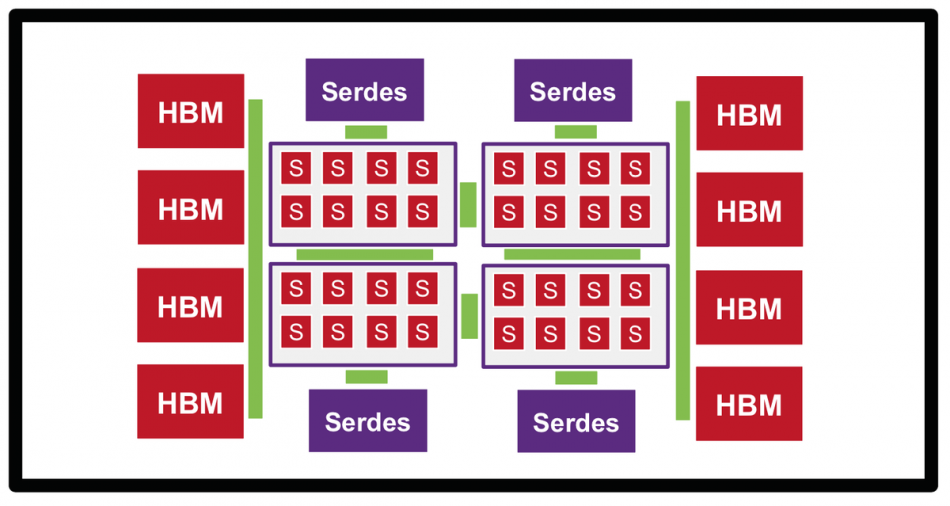
Image A device with multiple HBM stacks, CPU and I/O chiplets could easily contain more than 100 chiplets (Source: Phil Nigh)
The CPU arrays, network I/O and memory controllers provide avenues for reuse across a number of designs. Though some network devices may favor low latency and queue flexibility over raw bandwidth, it’s possible that the number of different physical designs may be quite low. For more than half a decade, Intel’s FPGA group has used chiplets, connected to the main programmable-logic device, to make it easier to tune the serial I/O options for different products and use older processes with better analog properties in doing so. That removes the cost of porting complex mixed-signal circuitry to potentially unsuitable nanometer-class process nodes.
Reuse options
“Sparingly using the most current wafer node and using older node as much as you can: that’s the main driver,” said David Hiner, senior director of advanced package technology integration at Amkor.
Intel principal engineer Robert Munoz argued: ”Reuse is key to portfolio-cost economics.” Chiplets provide the path to lower portfolio costs, at least in principle thanks to the reuse they enable. ”Especially important is the notion of project cost: you can have more configurations with fewer elements.”
Right-sizing designs can also play into lower costs, Munoz said. ”We can ship less wasted silicon because we need only populate the package with silicon customers want rather than shipping a large chip and turning parts of it off.”
This degree of control could be crucial as the kinds of processor today used in cloud servers migrate into more energy- and cost-sensitive edge deployments. ”For edge solutions, I still want to be able to use underlying building blocks but I need to right-size them. But there are great software benefits to an approach that uses the same building blocks,” Munoz said.
At the high end, being able to make the devices big enough is an issue, with the limitations of lithographic scanners and their maximum reticle size coming to the fore. “The reticle is starting to get too small,” said Sandeep Bharathi, executive vice president of SoC central engineering at Marvell. That is an issue that is likely to get worse in the coming decade as EUV scanners move to higher numerical-aperture approaches. Imec expects that to result in a reduction of the maximum achievable reticle area.
Bigger chips, smaller reticles
Even within the reticle area, practical chip size is not getting larger. If anything, the opposite is true. As has been the case over the past few decades, random defect densities continue to make high yield on large die areas challenging. Chiplets provide a way to divide a large design into higher-yielding devices and go way beyond reticle size, even using interposers.
“If you look at scale of the bandwidths now necessary, you need to increase the size of the package: the packages are getting substantial for terabit switching,” said Bharathi.
Actually achieving the benefits is another matter. “It’s very easy to say but hard to do when you have to look at how architectures need to scale to a certain die size,” Bharathi added.
“There is no free lunch here. It’s important to understand the tradeoffs,” said Munoz. “There are tiling overheads. You need die-to-die interfaces, which consume area and power. And they can cost performance versus a hypothetical monolithic alternative, though that’s not always fair because you might not get viable yields with the monolithic or even fit on a reticle. Chiplets aren’t going to be optimal in all cases. In some cases might be a sweet spot where monolithic makes sense.”
On top of those costs are incremental package, assembly and test costs for designs that may ultimately involve ten or even more than a hundred individual chiplets. “Inventory management can be more costly and complex. If you are integrating die from third party partners, you have to worry about margin stacking and inventory carrying costs,” Munoz noted.
An open market?
There are big questions over whether chiplet adopters will be buying large numbers of devices from third parties rather than using the architecture to maximize internal reuse. Phil Nigh, distinguished member of technical staff at Broadcom, asked, “What will the chiplet market look like? Ten years from now will there be a catalogue and you plug-and-play using components from that. Or will it be an evolution of what it is today, where an integrator works with a small number of trusted partners? Where they stay within the club and only go outside the club if they need something specific. It will probably stay like that for the next eight to ten years.”
Jawa Nasrullah, former president and CTO of zGlue said the industry needs to look at standards for chiplet-based design across multiple domains. He pointed to work in the OCP’s Open Domain-Specific Architecture (ODSA) that highlighted the importance of data exchange just for bus and serial interfaces between chiplets. Overall, chiplet-based packages will call for existing formats used for multichip module data exchange to evolve to suit 3DIC designs and to be used alongside formats that describe thermal and electrical behavior, perhaps drawing in existing standards such as Ibis for I/O modelling. “One particular standard we are excited about is ECXML, with provides thermal data in a machine-readable format,” he said.
Whatever the shape of the market, the differences with chiplet-based design call for major changes from the approaches used for monolithic SoCs, said TechSearch International president Jan Vardaman, “We need to change from silicon-centric thinking to system-level planning. It’s a mindset change. The industry needs to think about chip design in a new way.”