Nvidia proposes split-level link for chiplet interconnect
Nvidia revealed at its Fall GTC work the company has done on a bidirectional energy-saving chiplet interconnect that could hit the equivalent of 50Gbit/s per line.
In his talk on recent work performed by Nvidia teams, vice president of research Bill Dally described how they went back to work he and colleagues published several decades ago while at the Massachusetts Institute of Technology (MIT) to try to find a simple and energy-efficient high-speed interconnect for chiplets.
The problem Dally said was to find an interconnect suitable for interposers and organic substrates that does not impose a high overhead due to symbol encoding but which can support the datarates envisaged for processor complexes in multichip modules. Referring to estimates put together for the 2021 International Solid State Circuits Conference (ISSCC) by Walker Turner, Nvidia senior research scientist, Dally pointed to the need for 800Tbit/s of aggregate inter-chiplet bandwidth by 2030.
“With a switch chip of 25 x 32mm and using 90 per cent of the periphery for [the interconnect interface], we get the need for 15.1Tbit/s per millimeter around this perimeter to match this demand,” Dally said. “If we had a 50-micron bump pitch, which is what we’re facing about now, we would need 70Gbit/s to do that. But we anticipate scaling to a 40-micron bump pitch in this timeframe. So the real requirement is to have each of these signal lines, if they are single-ended and differential, each need to be operating at 50Gbit/s.
“It’s got to be a compact design. We don’t want a big tax on breaking our designs up into chiplets. And we want to make this a very low-power design. Our approach to making it low power is to build a simple circuit and the simplest circuit we can possibly build is a CMOS inverter,” Dally added.
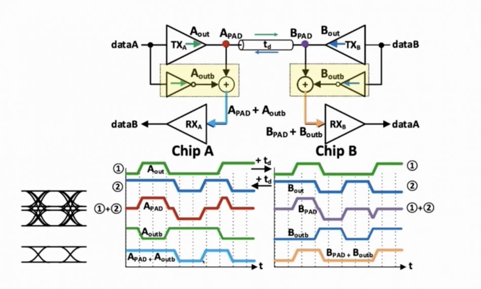
Image Diagram of Nvidia's SBD interconnect circuit and signalling
This focused attention among the team on traditional NRZ signalling, though this would call for a high clock rate. Moving to PAM4, as used by high-speed ethernet now, would drop the baud rate by half. But this complicates the circuit design and leads to problems such as increased inter-symbol interference that needs to be corrected. The approach the team settled on for this experiment was to turn to a split-level NRZ scheme from the work at MIT, in which the same line is used for bidirectional traffic. One direction takes the upper voltage range and the other the lower. Because of the inevitable near-end crosstalk, decoding at either involves subtracting the transmitted pattern, with a delay to match the received clock edges, to reveal the NRZ pattern sent from the other end.
The difference between the older and the more recent work is that the team was able to dispense with the differential amplifier in the original paper. “That amplifier is power-hungry, expensive, and difficult to make completely linear,” Dally explained. “It turns out the right way to do this is incredibly simple: use a passive resistor network to do the subtraction. We need a dummy RC network to kind of match the characteristics of the line but we can get by with just an RC network.”
There is a training process needed at start to adjust the parameters of the network using trimmers. The team tested the system on a 5nm process production chip where circuitry was used to mimic the characteristics of an interposer and its interfaces. “We build these big GPUs and switches and very often the fundamental pieces of silicon area aren’t completely used. In this case we used one piece of that silicon area to build two of these 16-lane PHYs – although we only connected 20 of the lanes – running over a 1.2mm channel,” Dally explained.
The tests showed that the Simultaneous BiDirectional (SBD) signalling technique can achieve low error rates with a maximum eye opening of 0.6 UI. “We have an extremely high timing margin and the received jitter here is under a picosecond,” Dally said, adding that the energy of transmission works out to be 0.3pJ/bit which assuming later tests can hit the datarates anticipated could work out to be an order of magnitude more efficient than existing proposals for chiplet interconnect.
“I’m really excited about this technology because as we go forward, we’re going to be building our systems out of many chiplets combined on interposers. And it’s really critical that we have the ability to get very high bandwidth between these triplets at very low energy and a very low area tax,” Dally said.