Macronix proposes 3D to breathe life back into NOR flash
NAND flash seems tailor made for 3D integration partly because it needs less interconnect for the array than other flash architectures. NOR, though far easier to use because of its random addressability, has been left far behind. But at IEDM this year, Macronix showed work that may bring back NOR, which stopped scaling a decade ago with the 4Xnm generation, as a mass-memory contender that can use 3D integration for scaling.
Hang-Ling Tue and colleagues at the memory maker does not use a NOR architecture directly. Instead, it applies a circuit approach that dates back to the early days of flash to provide bit-level access: the AND architecture. That is then applied to a stacked process that is derived from existing gate-all-around (GAA) 3D NAND structures.
Like typical 3D NAND memories, the stacked cells are formed by punching holes in a multilayer sandwich of oxide and nitride layers and then filling the deep holes. But rather than a homogeneous cylinder of polysilicon, Macronix’ experimental architecture is formed from several distinct plugs. Two of them are N+ doped to act as the source and drain of multiple stacked transistors, separated by a silicon nitride insulator column in the middle. The remainder of the polysilicon plug acts as a split channel.
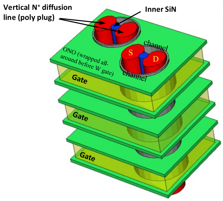
Image The structure of the Macronix 3D AND flash
In the resulting AND-type structure, each transistor has a paired source line and drain-connected bitline running orthogonally to the word line. The source lines are separately decoded rather than there being a common source. The polysilicon plug connects the sources and drains of the transistors in each stack. To operate like a NOR device, the structure needs to adopt some circuit-level and programming techniques but the team claims the architecture has demonstrated the basic feasibility of the approach.
The initial work was on an eight-layer structure but the team has done work on a 34-layer stack that appears to be viable. Above 70 layers, the NOR-style flash proposed by Macronix would challenge two-layer crosspoint phase-change memories at 20nm half pitch, they argue. Further improvements could come from ferroelectric transistors that would allow lower voltage operation and faster write speeds.