Integration forms highlights of upcoming IEDM
Different forms of heterogeneous integration take center stage at the IEEE International Electron Device Meeting (IEDM) in December this year.
To be held at the Hilton Hotel, San Francisco from December 7 to 11, 2019, IEDM will feature alongside a paper from TSMC on its 5nm platform an 3D heterogeneous integration scheme developed by Intel and papers on embedded MRAM and silicon photonics.
One of two Intel papers on heterogeneous integration is the latest in a series of bonded-wafer papers to appear at IEDM that home in on the problem of fabricating high-mobility NMOS and PMOS channels—crystal orientation across a wafer tends to favor one over the other. One solution, that has been the subject of papers from companies such as IBM and Intel, is to combine devices from two wafers in a layer-transfer process. Whereas the NMOS devices are built using conventional silicon processes, the PMOS transistors use germanium-on-silicon. This latest paper takes the idea a stage further by fabricating gate-all-around Ge-channel PMOS devices and then bonding them to the silicon wafer before cleaving the base of the transfer wafer away. Intel claims the PMOS device demonstrate the best Ion/Ioff performance of any Ge-channel devices so far.
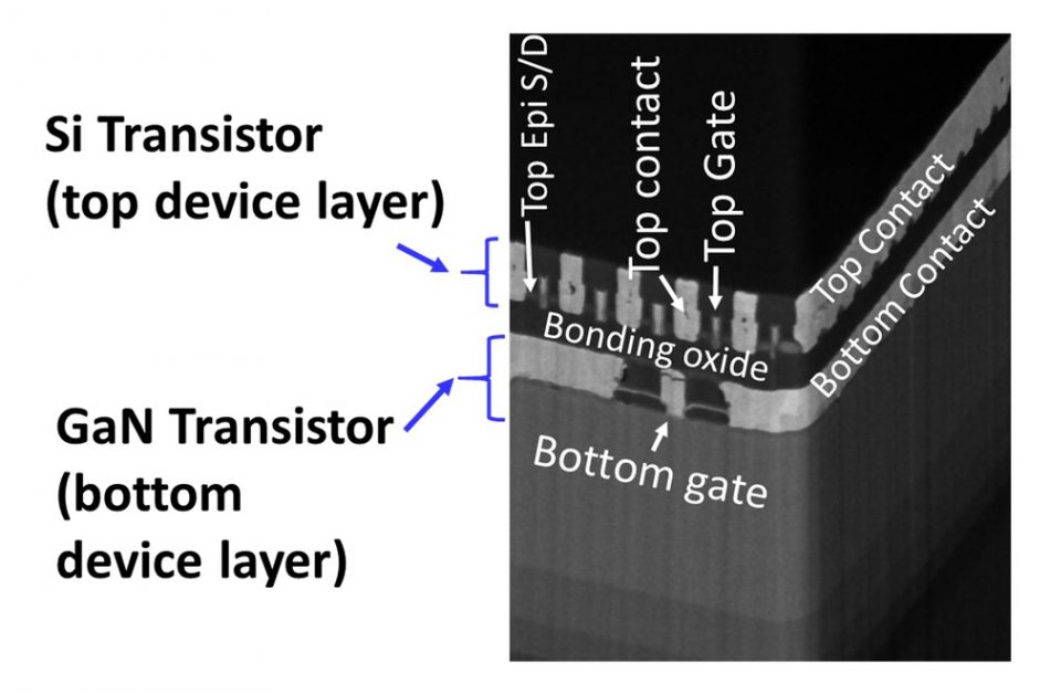
Image Cross-section of Intel GaN/silicon bonded wafer
The second 3D-integration paper is aimed at power delivery, RF, and SoC applications using gallium-nitride NMOS and silicon PMOS transistors. The first layer has the GaN transistors; silicon devices are built on top of those using a layer-transfer process. The GaN transistors demonstrate the ability to operate at millimeter-wave frequencies up to 7GHz. Silicon PMOS transistors offer a current drive of 0.85µA/µm and an off-current of 150pA/µm.
Focusing primarily on power converters, an Imec team will describe a monolithic GaN-on-SoI process, used to build a complete buck converter with the ability to switch 200V at 1MHz. The researchers used SOI to control back-gate effects and other parasitics.
For non-volatile memory integration, TSMC engineers will present a paper based on spin-torque transfer MRAM devices on 22nm CMOS that can survive six solder reflow cycles and which operates over a -40°C to +150°C temperature range. The researchers claim the reflow resistance can be traded off against performance to achieve 6ns read and 30ns write times.
A team from STMicroelectronics will describe a silicon-photonics technology built on 300mm SOI wafers that supports optical channels running at up to 100Gb/s. The process is able to form 60GHz photodiodes and high-speed phase modulators as well as silicon-nitride waveguides they claim offer high coupling efficiency than previous approaches.
In its paper on a 5nm platform, TSMC claims to achieve a logic density scaling of 1.84x over the previous process together with a 15 percent speed gain or 30 percent power reduction. The process makes extensive use of EUV lithography, helping to reduce the number of mask steps compared to the current 7nm technology. In a PAM4 transmitter test circuit, the 5ns process demonstrated speeds of 130Gb/s with 0.96pJ/bit energy efficiency. TSMC claims the process will be ready for volume production in the first half of 2020.
Before the conference sessions kick off, the two keynotes, delivered by ASML president and CTO Martin van den Brink and Intel senior fellow Robert Chau, will look at the future for process integration from two different viewpoints.