IoT and RF ‘to drive FD-SOI adoption’
The FD-SOI technology developed by CEA-Leti and STMicroelectronics is beginning to gain ground as chipmakers investigate the process as a way to deliver low-energy SoCs and wireless communications more cheaply than finFET-based alternatives.
Since January, a number of major companies have said they are either testing the technology or plan to adopt it. Over the past couple of months, Ciena, Cisco, Freescale Semiconductor and Sony have said they plan to develop devices using 28nm FD-SOI or at least investigate the possibility.
At Embedded World in Nürnberg late last month, Geoff Lees general manager of Freescale’s microcontroller business unit, said energy efficiency is key not only to the company’s 32bit microcontrollers but to applications processors, such as the iMX family. “Our objective is to go to an ultralow leakage 28nm process where we can see a common path for our microcontroller technology as well as the application processor technology. We see 28nm FD-SOI as the ideal opportunity to bring those roadmaps together and create a larger scale for the solution that we invest in.
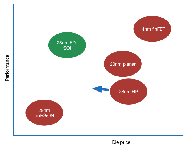
Image Performance and die price comparison - derived from chart presented by Gerd Teepe
“We have the potential to reduce leakage and power consumption to the kind of levels that we see as needed by microcontrollers. If you don’t maintain that stretch, it will be difficult to maintain compatibility in terms of the power envelope needed by the market going forward,” Lees added.
’The IoT process’
“FD-SOI is the technology for the IoT,” Lauren Remont, vice president of technology and product strategy at ST, claimed in a keynote speech at the DATE conference in Grenoble (March 10). “For IoT, it will provide very low power and there are derivatives going on that will optimize RF, provide ultra-low voltage and add embedded non-volatile memory.
“We have made a lot of progress in the ecosystem. Companies such as Sony, Freescale and Lattice are adopting FD-SOI,” Remont added, also pointing to the addition of SunEdison as a wafer supplier in addition to original provider Soitec, as well as the support of design houses such as eSilicon and OpenSilicon.
Remont pointed to application areas such as wearables and automotive as being potentially big targets for FD-SOI. He described work on one project to cut power consumption on a smartwatch SoC from 34mW to 10mW in a shift from 40nm to 28nm FD-SOI. A second project to optimize the design for FD-SOI would halve the power again, he claimed.
Automotive applications can make use of better radiation hardness as well as power consumption, Remont argued. “If you look at video analytics for a smart car, it’s a safety critical and power limited. The target is just 3W. In conventional technologies, you need to double key blocks to check their behavior in case of single event upsets. Thanks to the lower soft-error rate of FD-SOI you can avoid the need to have this redundancy. That’s true for the core and the embedded memory. It has benefits in both cost and time to market.”
The shift to FD-SOI initially reduced consumption from 5W to 4W. “We are working to reduce that to 3W,” Remont said.
Alternative path
Gerd Teepe, director of design enablement for GlobalFoundries, said 28nm FD-SOI offers an alternative path for design teams that do not want to move to finFET. “28nm is probably the last node where you can use single patterning. As long as we don’t have EUV ready, for the smaller geometries, the transistor price is going back up again. FD-SOI at 28nm pushes performance back up and simplifies the production technology. In FD-SOI everything simplifies because problems, such as dopant fluctuation and the variation it causes, go away.”
To try drive adoption, at least within Europe, the European Union has set up programs such as Things2Do. “The aim is to create a local European ecosystem,” said Blouet.
Much of the promise on power consumption involves the use of advanced design techniques such as active body biasing, where tool support is currently scarce. However, companies such as Sony and ST have been able to demonstrate its applicability to energy saving using a combination of existing tools and scripts. “We have deals between ST and the big EDA companies to implement in tools this capability,” said Blouet. “We showed that it is possible to implement ARM’s Big-Little concept using just a single core. It opens an area in terms of architecture that’s not fully investigated yet.”
Although CEA and ST are working on an enhanced RF variant process that will take Fmax to 350GHz, Olivier Thomas, CEA-Leti design center project leader, said a paper at the last International Solid State Circuits Conference (ISSCC) showed that RF designs are feasible using the standard process, which would help propel the process into IoT SoC projects.
Teepe said: “FD-SOI is capturing mindshare across Europe. That’s something that’s different from the past. We see that there is a real European momentum developing.”