Oxide DRAM gains traction at VLSI Symposium
The VLSI Symposium on Circuits and Technology in mid-June will show the rapid development taking place in oxide-based replacements for traditional DRAM cells as well as the emerging area of memory-based low-power machine learning.
At this year’s conference, taking place in Honolulu from June 13 to 17, 2022, a session has been set aside to cover progress in transistors based on the material indium gallium zinc oxide (IGZO). Originally developed as a thin-film transistor material for flat-panel displays to take advantage of the transparency of indium and zinc oxides, the material has proved to be a contender for transistors that can be implemented in the metal stack above conventional silicon circuitry.
Gosia Jurczak, Lam Research managing director in Europe and program chair of the VLSI Symposium, said because IGZO-based transistors showed low leakage current the material started to be considered as a contender for memories in situations, such as the back-end-of-line (BEOL) metal stack or in vertical structures where the use of silicon would be far more difficult to employ. At the International Electron Device Meeting (IEDM) in 2020, Imec researchers showed that the material could used in capacitorless embedded DRAMs, with potential as 3D stacked memories.
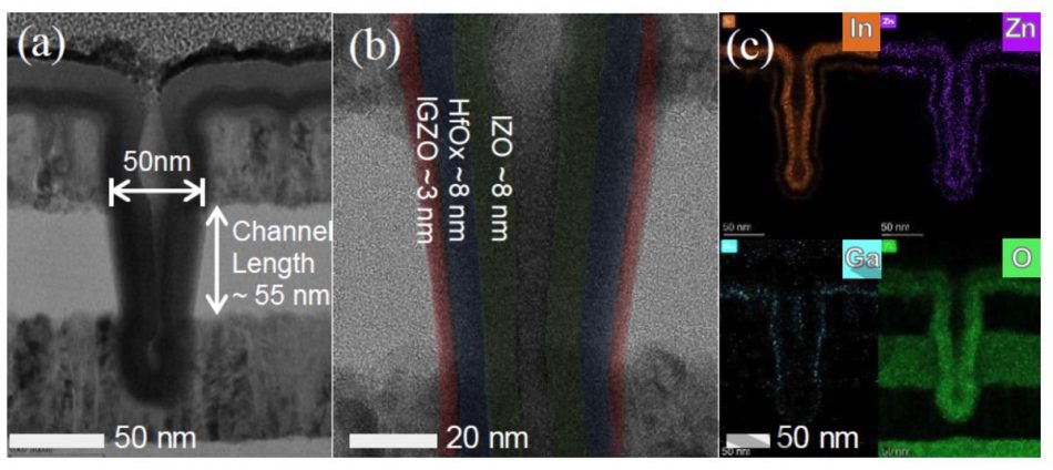
Image Huawei's channel-all-around IGZO transistor cross-sections
At this year’s event, a team from Huawei will report on a vertical, channel-all-around IGZO transistor with an active footprint of 50x50nm2. The indium-based oxide surrounds a cylinder of hafnium oxide – which was shown to be an effective gate oxide for IGZO in 2019 by the University of Tokyo – which encapsulates an indium zinc oxide electrode. The channel length of the vertical device is 55nm and delivers a current density of 32.8µA/µm with a threshold voltage of 1V and a subthreshold swing of 92mV/decade. The team claims the FET is a promising candidate for 3D DRAM beyond the 1a nodes. Working with Huawei, a group from the Chinese Academy of Sciences has developed a compact model for these channel-all-around devices in order to gauge their susceptibility to bias temperature instabilities that might limit the lifetimes of these memory cells.
Other papers on IGZO at the conference will include a presentation from Imec which focuses on a raised source-drain structure for two-transistor, capacitorless (2T0C) DRAM cells. These deliver a current density of more than 30µA/µA at a lower threshold of 0.3V and an off-current of around 4×10-19.
Looking at logic applications, a group from the Chinese Academy of Sciences claim to have shown IGZO FETs can scale down to a channel length of 30nm using a dual-gate structure to achieve a subthreshold swing of just 63mV/decade. Using a bottom-gate structure, University of Singapore workers scaled down the transistor even further, to 12.3nm with the help of lift-off manufacturing technique.
Another key characteristic of oxide FETs is their demonstration of ferroelectric behaviour, an avenue pursued by University of Tokyo researchers in their work on IGZO. Another group at the university will show how hafnium zirconium oxide insulating films integrated into a silicon transistor can be applied in an machine-learning accelerator. The polarization dynamics of ferroelectronic memories, which show a clear hysteresis in the transition between the 0 and 1 states, make it possible to get the cells to perform compute operations using reservoir-computing techniques.
One of the issues surrounding analog compute-in-memory accelerators is their requirement for comparatively large arrays of analog-to-digital converters (ADCs) to extract results. A team from the Georgia Institute of Technology has developed an ADC-free accelerator based on resistive memory (ReRAM) materials. The cells perform direct digitization – using the time it takes to charge a load – of results computed in the analog domain, resulting in a halving of the area needed for sensing circuitry and increasing effective throughput almost seven-fold.