Combined database underpins 3DIC design suite
Cadence Design Systems has built a unified database to support a group of tools to support the planning and implementation of 3DIC system-in-package (SIP) designs with a focus on high-end computing and hyperscaler projects.
The core of the Integrity platform is a database built on top of the structure developed for the Innovus IC-design portfolio. Vinay Patwardhan, product management group director for digital and signoff, said the database uses a hierarchical architecture to accommodate IC designs that target different processes and which need to be integrated into a 3DIC stack or a hybrid of 2.5D interposer and 3DIC stacks. The database combines layout information imported as LEF files from the various chips or chiplets that will comprise the final design.
Although production is today largely restricted to HBM memory stacks and specialized products such as image sensors, Patwardhan said the company is working with 20 organizations that are looking to expand 3DIC into memory-on-logic at least to the level of prototype development in the expectation that this will become a mainstream option on the way to logic-on-logic 3DIC stacks.
“There is a big demand from hyperscalers. The demand on memory bandwidth in their designs is so high that they are looking at new architectural configurations and system-level innovation,” Patwardhan said. At the same time yield issues in many of the designs that need large die sizes is hurting cost-effectiveness. Moving local memories off-chip cuts the die size but hurts bandwidth because of the length of the interconnects needed. If those memories can be moved to a second die mounted on the first, the interconnect can stay relatively short and manufacturers can take advantage of the yield benefits of using two chips at roughly half the original size.
Partitioning support
One aspect of Integrity is support for the floorplanning and layout of logic and SRAM split across two stacked chips. This, Patwardhan claimed, takes advantage of Innovus’ ability to mix macro and standard-cell placement. The idea is to have a starting point of a 2D design that includes all the SRAM macros on one die. These are then moved to a second die that is assumed to be stacked on top and the layout engine will tune a layout to minimise the connection distance between the individual macros and the logic elements that access them. In its current implementation, the assumption is that the logic and memory slices will be aimed at the same process. However, the company envisages being able to perform partitioned floorplanning where the memory macros are implemented on a different, possibly older technology than the logic, taking advantage of the fact that memory has not scaled as well as logic on recent nodes. The stacked design, in principle should boost frequency, cut power, or both.
“Some of our customers are running really high-performance cores. They are trying to push frequency without making too many changes to the underlying architectures and without increasing power,” Patwardhan said.
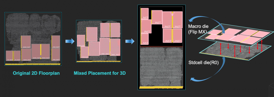
Image Parallel macro and cell placement supports split logic-SRAM chips in a stack
Once the planning element has created a workable floorplan, the chips are divided and put through a detailed implementation flow. When this has completed, static timing analysis can be performed across the stacked chips. Because the logic spanning the chips in a stack will typically not use serialization protocols or active buffers to minimize latency, timing analysis needs to act on circuits that span more than one piece of silicon. This potentially increases the number of corners that need to be used to sign off timing dramatically. Although some teams may try to confine the number of paths affected by this by using signalling protocols similar to those used for 2.5D-based projects, the company has developed several techniques intended to cut down STA runtimes by checking for redundant calculations when the corners from different chips are combined.
Further additions to the Integrity product are support for thermal and IR-drop analysis as well as a cockpit view used to plan aspects of the design such as bump and contact-pad layouts.
Among the early adopters who have disclosed their use of the Integrity tools are Imec, photonic AI-accelerator specialist Lightelligence, and China-based SaneChips, which is looking to build interposer-based stacks for hyperscale and 5G systems.