Boost your DFT efficiency for AI silicon design
The market for artificial intelligence (AI) silicon is highly competitive. AI compute requirements are doubling every 3.5 months, and there are at least 75 startups and established chip design houses competing for business.
This places inevitable pressure on reducing the time and resources needed to execute all parts of the design flow, including design-for-test (DFT). A new technical article discusses strategies that can be used to shorten DFT and make it more precise in the context of the Tessent platform from Mentor, a Siemens business.
‘AI chip DFT techniques for aggressive time-to-market’ discusses hierarchical techniques under three headings:
- Exploit AI Chip Regularity
- Perform DFT insertion at RTL
- Eliminate DFT-to-test insertions
These area applied in the context of three common factors across AI designs. They are large chips with billions of gates. They typically replicated many processing cores. They have distributed memories.
Exploiting regularity
As figure 1 shows, DFT tasks at different levels can be conflated to sign off multiple parts of the design as appropriate based on insertion, pattern generation and verification at each.
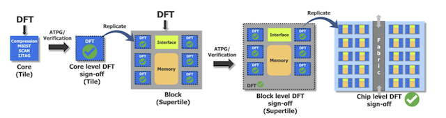 Figure 1. Tessent hierarchical DFT allows for complete DFT sign-off at different levels of design hierarchy.
At the core (tile) level, designers and test engineers can, for example, implement ATPG and scan test pattern verification across groups of cores (saving the need to implement test repeatedly across instantiated cores, and the resulting area penalty).
This same kind of grouping and implementation – with much the same benefits – can then be addressed at a ‘block’ hierarchical level (supertile) for interface logic and memory.
Finally at the chip level – the point at which all these tasks would have been addressed – a more efficient whole-chip signoff can be undertaken.
“Exploiting the AI chip regularity for DFT implies that all the DFT work – including test insertion, test pattern generation, and verification – is completed just once at the core level,” explains author Rahul Singhal. “The complete, signed off core is then replicated automatically to complete the chip-level DFT implementation.”
He also describes how this approach allows for a greater exploitation of the inherent qualities of IJTAG, as well as options for channel broadcasting (sending the same test data to identical groups, reducing time and test pins) and the use of shared memory BIST controllers.
DFT insertion at the RTL
Performing simulation, debug and verification at the gate level is potentially very time consuming, particular because of the consequent need to reiterate synthesis. Singhal proposes using capabilities within Tessent to move insertion from its traditional locus to the RTL (Figure 2).
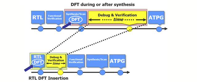
Figure 2. Avoid traditional gate-level insertion (Mentor)
“DFT insertion in RTL mitigates these issues because any DFT changes can be verified and debugged faster in RTL without the need of going through the synthesis step, he writes. “It is equally important to notice that RTL DFT insertion also allows for early I/O and floor planning of the chip. This process significantly shortens the design development cycle.”
Eliminating insertions
This stage exploits specific qualities within Tessent SiliconInsight which allow DFT engineers to undertake silicon-bring up themselves. Moreover test engineers can run diagnosis in resolutions from flop-level to net-level without the help of DFT engineers.
“This solution speeds-up the entire process by eliminating the time-consuming and costly iterations between DFT and ATE domains,” writes Singhal.
He also describes the two available variations of SiliconInsight : Desktop, and ATE-Connect.
By using RTL-based hierarchical DFT in conjunction with SiliconInsight, Singhal asserts that, “Users have achieved up to 10x faster test pattern generation with 2x pattern reduction using 10x less system memory.”