Imec stacks transistors for denser 3nm option
Imec has proposed using stacked CMOS transistors to improve density for the 3nm generation.
In a presentation at VLSI Symposia 2018, Anda Mocuta, head of Imec’s team working on advanced CMOS technology, said the push to stack the two halves of the basic CMOS inverter on top of each other comes from issues scaling the distance between n-channel and p-channel transistors within standard cells. The result is the ‘complementary FET’. Mocuta said the approach would make it possible to continue the recently adopted trend of reducing standard-cell track heights.
The stacked architecture would make it possible to have just two or three tracks within the cell. In addition it offers the ability to compress SRAM cells more than would be possible with pure 2D scaling. “You can get about a 40 per cent gain in area by using CFETs in SRAM cells as well,” Mocuta claimed, adding that the approach can help reduce the amount of 2D local wiring needed in commonly used standard cells in favor of more lithography-friendly simple 1D connections. “We think the biggest advantages are in connectivity. The minimum height of an SRAM is about eight fin pitches and 2xCPP wide.”
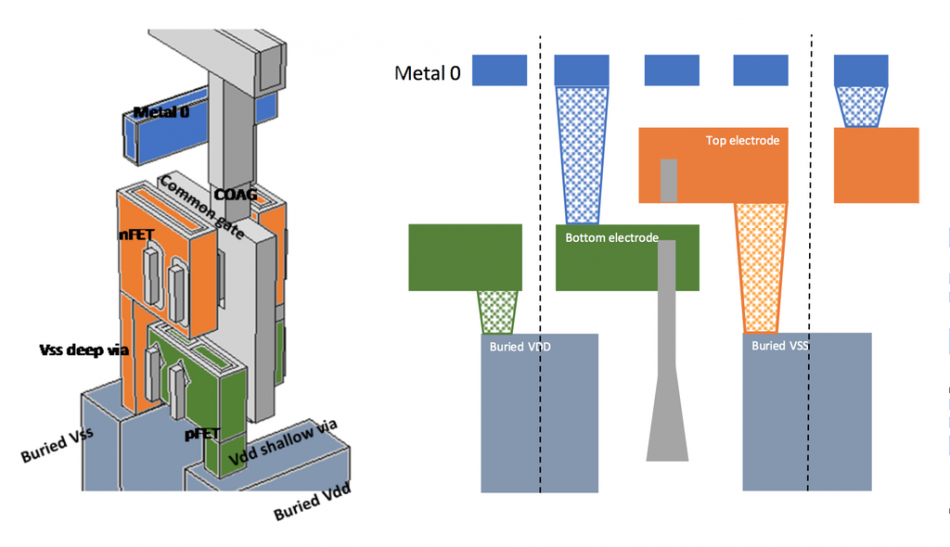
Image Projection and cross-section of a finFET-based CFET
The CFET architecture does just not involve changing the way n- and p-channel transistors are arranged but the power-rail architecture as well. “A buried power rail is a requirement and an enabler for this,” Mocuta noted. To keep resistance for high-current connections down, Imec proposes using ruthenium for the power rails and for the longer vias that will be needed to connect the lower transistor to middle-of-line (MOL) routing. “The via resistance is the biggest contributor to device resistance.”
Mocuta claimed the CFET architecture provides the ability to use a variety of transistor designs, recognizing there may be a need to move on from finFETs by that time. “You can have a nanowire on nanowire, nanowire on fit, nanosheet on nanosheet. All are possible and may come in at any point. But this work focuses on fin on fin,” she explained.
In simulations put together in co-operation with Coventor and Tokyo Electron, the Imec team assumed for their experimental 3nm CFET process a contacted poly pitch of 42nm, and a pitch of 24nm for the fins and for the bottom metal layers.
Imec developed a process flow that is intended to balance the issues of thermal budget with performance. Mocuta said the nature of the process makes the top device “SOI-like”. She added: “We have worked on a process flow that has borrowed heavily from a gate-all-around flow. The processing of the device is not much longer than a regular device. But the tolerances will be much tighter. Control of the bottom contact in particular is critical. The key issue will be the process tolerances. But we can meet or even surpass finFET performance.”
In the version proposed at VLSI 2018, the connections from the supply network to the buried power rails are using long vias from the top surface. Mocuta said the use of buried rails makes it possible for chipmakers to consider implementing the power grid on the backside of a thinned wafer. In doing so, they could both free up signal routing and take advantage of a denser power grid to help deal with IR drop issues.
Some observers at the conference noted the buried power rail could be adopted without moving to the CFET architecture, which may face challenges from the manufacturing tolerances required and the continuing challenge of issues with thermal budgets for stacked-transistor processes. Following this round of simulations, Imec intends to fabricate experimental wafers based on the 3nm CFET architecture.