Early package assembly verification for faster, better results
Early package assembly verification allows engineers to catch issues quickly, when they are easier to fix. But it requires a through understanding of the multiple chiplets that make up today’s 2.5D and 3D designs.
The process also requires a tool infrastructure that can evolve as component choices mature through either addition or replacement.
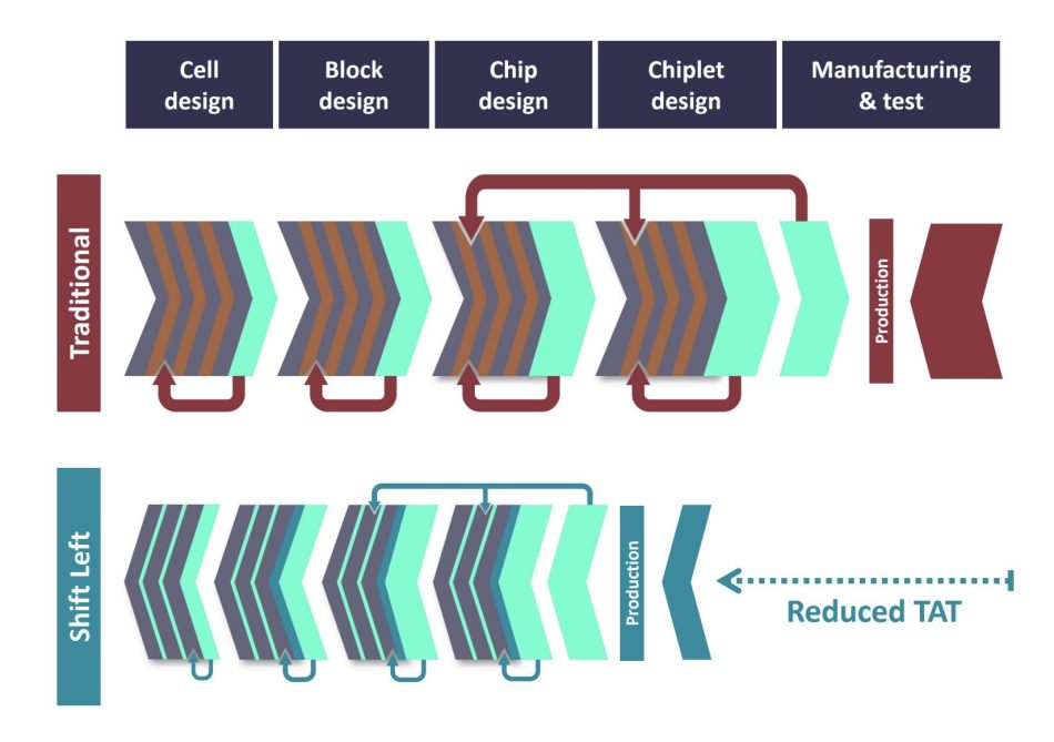
The results of this signature ‘shift left’ strategy are greatly reduced verification runs and simpler debug.
A Siemens EDA technical article, Reduce 3D IC design complexity with early package assembly verification, considers that challenges designers face and charts the path to a full 3D package integration flow within the context of the Calibre physical verification and Xpedition families.

Figure 1. Calibre Shift Left design solutions enable design teams to enhance productivity and design quality while reducing time to market (Siemens EDA – click to enlarge)
It notes the ways in which 2.5D and 3D design already diverge from traditional design flows, and are likely to continue to do so as best practice improves, while capturing the current state-of-the-art in package assembly verification.
The content is designed to be of general interest to IC and SoC designers looking to stay on top of the latest in semiconductor system design, but will be of particular value to three groups:
- Chiplet designers seeking to enhance chiplet integration and performance.
- Package layout designers aiming to optimize 3DIC layouts.
- Thermal mechanical engineers focused on addressing stress and temperature concerns in 3DICs.
“It’s clear that true 3D IC analysis and verification requires comprehensive knowledge of the entire system at the detailed level of each component,” writes author John Ferguson. “By enabling such an environment early in the assembly flow, not only is the verification approach itself greatly simplified and made faster, but also an innovative approach for multi-physics challenges can be accommodated.”