How to automate pre-tape-out ESD protection verification
Reliability verification can largely be addressed during library development at the device- or gate-level. But not always. For designs that are highly complex, operate across several power domains and/or target an advanced process node, the reliability challenge shifts to the interconnect.
Here, even as familiar a task as protection verification for electrostatic discharge (ESD) can become difficult. A new paper from Mentor, a Siemens business, describes a methodology that automates this type of verification at the full-chip level. It offers a new approach to ESD verification at the chip assembly stage before tape-out, something that even today is often done by manual inspection.
In some cases, manual strategies have continued to be preferred to preserve competitive advantage, given how difficult the task is. At the same time, the lack, until now, of an EDA methodology has also led foundries to publish many ESD guidelines only as text descriptions. Current strategies raise obvious risks of respins and delayed time-to-market, so automation is now vitally needed.
At the heart of Mentor’s proposed approach is a move to a rule-based logic-driven layout static approach that enables a methodology using context-aware checks. Author Frank Feng, Circuit Verification Methodologist at Mentor, says this will check “not only for the existence of ESD protection circuits, but also the robustness of the interconnect used within these circuits to effectively transport the energy of an ESD event”.
The paper describes methodological implementations for use in the context of Mentor’s Calibre PERC reliability platform and the two primary processes.
- Verifying ESD protection circuits exist.
- Verifying ESD current path interconnect robustness.
It describes the tasks that need to be carried out and now automated for ESD circuits in three locations.
- Those between I/O and internal gates
- Those between power and ground ports
- Those found across different power domains
Figure 1 shows overviews of the logic-driven layout geometric flow (left) and the logic-driven layout electrical check flow (right).
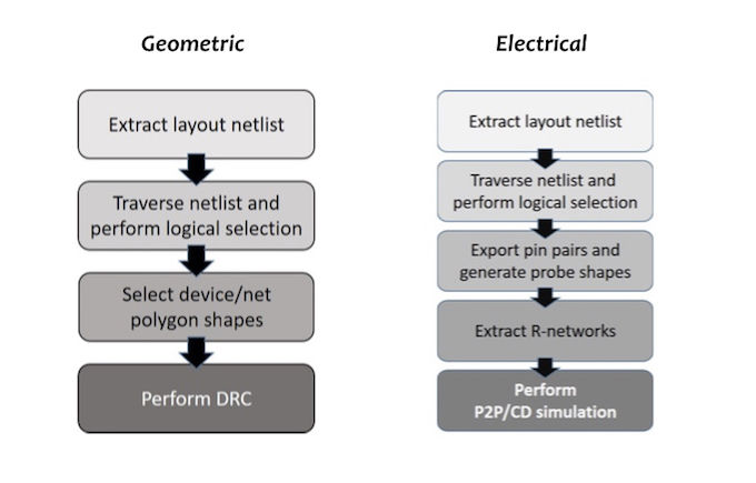
Figure 1. Overviews of logic-driven layout ESD verification flows for geometric checks (left) and electrical checks (right) (Mentor)
The methodology now, Feng writes, “enables foundries to develop and provide qualified ESD process design kits that cover a majority of ESD rule checks for chip-level tape-out.”