Machine learning and chiplets headline VLSI Symposia
Among the highlights at the upcoming VLSI Symposia are novel devices that use semiconductor properties to act as the building blocks for analog machine-learning systems alongside large-scale implementations of digital neural networks.
At June’s conference, to be held in Kyoto, Japan, Toshiba engineers will describe the use of ferroelectric tunnel-junction memristors in a reinforcement-learning system. The memristors allow machine learning to take place entirely in the memory array by taking advantage of a property that is normally considered a problem. The ferroelectric memristors exhibit stochastic switching behavior, which the researchers argue is beneficial in moderation as it lets a systems acquire a policy using a process similar to a random search. In simulations, the team claims the approach has successfully balanced a pole on a cart with better performance than deterministic algorithms.
Using a 16nm process and multichip integration of a 36-chip array, nVidia has built a prototype deep neural network (DNN) accelerator that achieves just under 128Top/s at an energy cost of 0.11pJ/op. The 36-chip device is able to classify 2615 images per second running the ResNet-50 benchmark. The company’s engineers claim the approach they have taken makes it easier to build scalable machine-learning arrays than traditional approaches based on monolithic architectures: different use-cases can be tackled by creating MCMs with larger or smaller arrays.
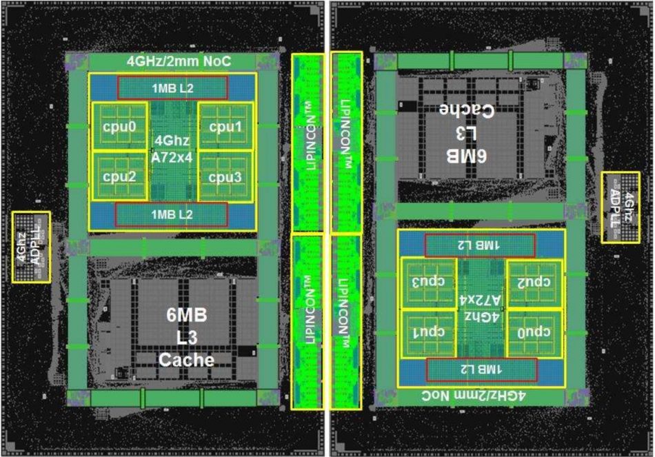
Image TSMC multichip module using internal LIPINCON interfaces
To enable denser MCMs, TSMC has developed a technique for stacking one chiplet on top of another at the fab rather than during the packaging phase. The company claims its System on Integrated Chips (SoIC) approach offers higher interconnect density and better energy efficiency for interchip I/O.
Based on its existing CoWoS technology TSMC engineers will also describe a project to implement a high-end multicore processor based on chiplets. The package contains two chiplets made using a 7nm process, each with four Arm Cortex-A72 cores operating at up to 4GHz. The chiplets communicate using an interface TSMC calls Low-Voltage-In-Package-INterCONnect (LIPINCON) that offers energy efficiency of 0.56pJ/bit and a bandwidth density of 1.6Tb/mm2.
To improve the bandwidth density of off-chip communications, Xilinx will present its work on a 50Gbit/s silicon-photonics link. Fabricated in 16nm CMOS, the transmitter and receiver elements employ T-coils to improve the modulation efficiency of the electro-absorption modulator and to reduce the noise of the transimpedance amplifier.
At the other end of the scale, a team from the Semiconductor Energy Laboratory will describe the use of a 60nm thin-film process based on indium gallium zinc oxide (IGZO) to create an processor for normally off computing. A microcontroller implemented using the process can retain data during power gating, storing data to backup memory in a single 21ns clock cycle. Restoration is slower at 4.5µs, largely due to the settling time of the integrated voltage regulator. The device is also able to achieve standby power of just 880nW thanks to the low leakage of the IGZO material stack.