ODSA weighs options for chiplet interconnect
The group within the Open Compute Project that is trying to promote a market in chiplets for server accelerators sees a combination of parallel and serial interfaces being important for interchip communication.
Meeting at Samsung’s North San Jose office at the end of March, the Open Domain-Specific Architecture (ODSA) group discussed progress on a proposed proof-of-concept multichip module (MCM) alongside possible inter-chip communication options and business-model challenges.
Bapi Vinnakota, director of silicon architecture program management at network interface specialist Netronome, said there are clear reasons for moving to MCMs for server accelerators. For one, there is the space issue as “accelerators tend to lead to larger die,” he claimed. In addition, “each accelerator will serve a smaller market than a general-purpose CPU. Both impact the economics of building accelerators. The answer might be to shift to a chiplet-based design rather than a monolithic design”.
Complex IP such as multicore general-purpose processors, I/O controllers and memory can be bought in as discrete chiplets and integrated on a laminate or silicon interposer. Doing it at package level should greatly simplify the interchip connections as they do not need the ESD protection or large I/O buffers of ICs that are expected to interface at PCB level. This supports much lower power consumption for inter-chip communications. Many use a chart compiled by DARPA to show the advantage. Chips separated by a matter of millimetres on a laminate could consume a few picojoules per bit versus the tens of picojoules required for PCB-level I/O.
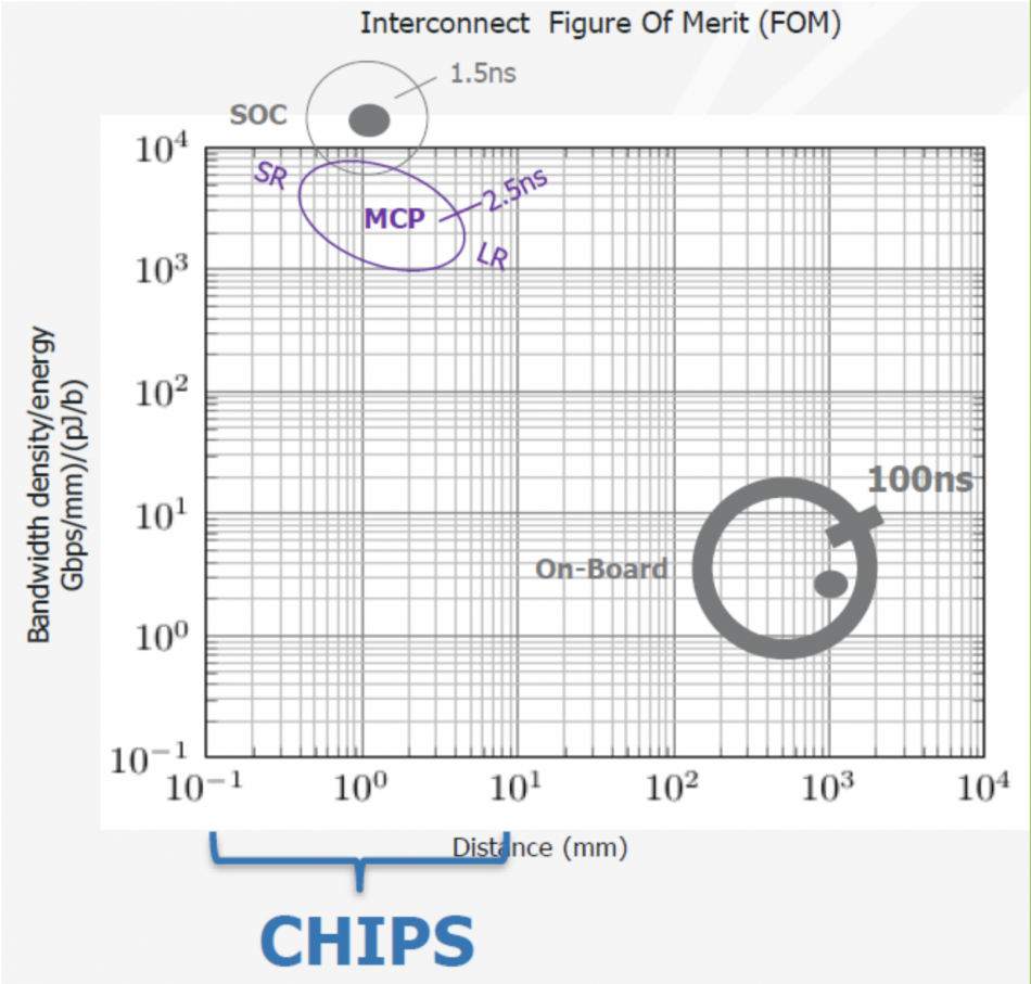
Image The ODSA is aiming for an energy sweetspot some way from PCB interconnect (Source: ODSA/DARPA)
The problem is defining interfaces that designers of these prospective chiplets can get behind. Up to now, most chiplet-based designs have been organised around the needs of single companies, such as Intel’s Programmable Systems Group or Marvell Mochi-based products. The ODSA initiative relies on an open market for chiplets developing. Ideally, the accelerator developers would coalesce on one or two clearly defined I/O formats in order to be able to choose from as many options as possible from third-party suppliers to round out their MCMs.
Greg Taylor, zGlue fellow, said the group had suggestions for seven possible interfaces to consider. Some of them are built around serial-I/O standards. Others for parallel buses, including the flexible but relatively unconstrained bunch of wires.
Mark Kuemerle, architect at GlobalFoundries and its ASIC spinout AveraSemi, said: “It’s very hard to convince yourself that any one type of interface is going to work with all various types of chiplet-based systems that are going to be used.
“There are some pointers towards the kinds of interfaces that are going to be used,” he added. “We are seeing a lot of traction for fast serial interfaces.”
Kuemerle said the 112Gb/s Extra Short Reach (XSR) serial interface developed for intrapackage interfaces inside high-performance computers and routers is becoming a de facto standard. “There are also some really novel USR [ultrashort reach] implementations,” he added, pointing to the work done by Kandou and its Glasswing technology that has been used by Marvell for the inter-chiplet communications employed in its Mochi devices.
A potential option for parallel interfaces that is already in use is Intel’s AIB, Kuemerle said, which the chipmaker has made available on a royalty-free basis. Intel uses AIB in conjunction with the EMIB technology to handle communication between core FPGAs and serdes I/O controllers in the Stratix products. Intel has claimed an energy density of 1.2pJ/bit for the first generation of AIB and a bandwidth density of 1.5Mbit/µm2.
The ODSA’s bunch-of-wires proposal may provide better energy and bandwidth density metrics. In practice, assuming the ODSA makes good progress with its principle, the bunch of wires is likely to be a lot more detailed than its name suggests. Already, members of the group have proposed signalling systems and options for test and power management that make it more than a simple point-to-point wire-level interface.
Turbo option
“The basic idea for the bunch-of-wires interface we are proposing is to start with a simple CMOS I/O buffer: think what chips used 20 years ago before serial came into our lives to give us cheaper PCBs,” Kuemerle said. “If we were trying to do this on a PCB it would be untenable. But we can have a lot more signal traces on a laminate. And by keeping everything on a laminate, we can reduce the ESD requirements. There is a very straightforward subset of AIB we could use to build backward compatibility into this standard.”
To improve throughput, Ramin Farjad described a scheme the ODSA group calls “Bunch of Wires Turbo” that combines several old electrical tricks. One is to run transmit and receive simultaneously to improve utilisation. The other is source-synchronous double-datarate transmissions similar to those used for memory interfaces. This would most likely support throughput per lane of 2 or 4Gbit/s and potentially higher with termination, at the cost of a few tenths of a picojoule per bit. “With termination, we could go up to 12Gbit/s on a wire and probably 5Gbit/s unterminated,” he claimed.
Voltage is another area of choice. It could go as high as 1.2V for compatibility with HBM. “But for many applications that’s probably too high. 0.9V would be compatible with AIB. There is a lot of interest in 0.75V and up. Lower voltages would help from a power point of view but the design is a challenge,” Farjad noted.
Based on a “pathological” activity level of 40 per cent, Farjad estimated sub picojoule per bit operation is possible with a 0.8V interface over a distance of 20mm.
“For low throughput, bunch of wires looks very attractive,” Taylor claimed. A speed of 2Gbit/s to 4Gbit/s would push the bunch-of-wires option into the useful range for designs that use buses like AHB, according to Farjad, with speeds below 2Gbit/s being insufficient.
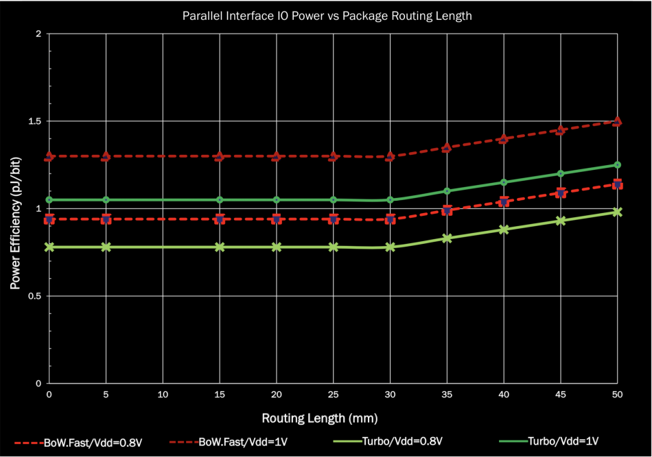
Image Energy estimates for unidirectional and bidirectional (Turbo) bunch-of-wires options
However, even with the Turbo option the bunch of wires may not be an option for accelerators where very high throughput is a requirement. Another issue is one of routability. “In principle, the bunch of wires is very straightforward but if you need to take a 500-wire parallel bus through a 90° turn, that’s not a pleasant thing to do,” Taylor said. This is where serial interfaces based on standards such as PCIe, USR or XSR may win out.
Although opting for a serdes-based interface is likely to improve throughput and routability, it comes with problems. The biggest potential stumbling block in accelerators is that of latency. XSR at more than 54Gbit/s is a particular problem because it relies on the multilevel signalling scheme of PAM4. Brian Holden of Kandou said: “This produces a whole load of errors. You can clean them up with forward error correction but that produces latency.”
Typical latency for error correction with PAM4 is on the order of a hundred nanosecond. Latency with Bunch of Wires Turbo, on the other hand, is just a couple of nanoseconds.
Taylor noted that a key design metric is likely to be one that focuses on the ratio of internal processing to external bandwidth required. High-intensity accelerators with commensurately high ratios might favour the bunch-of-wires approach whereas those components with the job of funnelling data at high speed to different units apply serial interfaces from the PCIe or LAN world. Latency considerations will probably play a major role in whether designers favour the LAN-derived standards such as USR or XSR over PCIe lanes or the simplicity of the bunch of wires.
Proof of concept
The proof-of-concept the ODSA group wants to build may provide clues as to how an open market in chiplets might develop. The current proposal combines a number of readymade devices that use older interface standards such as PCIe Gen3 for I/O. As these off-the-shelf devices largely focus on serial interconnects for I/O, beyond the memory interface, suppliers may simply choose to make those available in chiplet form rather than create specialised versions with parallel buses. Such buses would be reserved for designs that need ultralow latency between devices: maybe restricted to connections between custom accelerators. Connections to the third-party devices may be able to tolerate the higher latencies of serial I/O standards.
At the board level, the users will continue to employ serial interconnects. At the ODSA meeting, Facebook engineer Whitney Zhao described the work carried out in conjunction with Microsoft Azure and Baidu to develop a mezzanine interface for custom accelerators. At the electrical level, the connectors for the Open Accelerator Module (OAM) have been specified to operate at up to 112Gbit/s with PAM4 signalling. The format is designed to work with a variety of baseboards that can apply different interconnection topologies such as hypercubes and nearest neighbour based on which boards are plugged in. In these systems, the users expect the individual accelerators to be able to be tightly coupled. As a result, serial interconnections carrying through into the intrapackage links used by individual accelerator chips may prove to be acceptable.