Cadence tunes Virtuoso for 5nm and SIP
Cadence Design Systems has made enhancements to its Virtuoso mixed-signal layout tool at both the system-level and nanometer-design levels for its 18.1 release.
Yuval Shay, product management director for Cadence’s analog and custom-IC group said the latest release improves on the system-in-package (SIP) design support of last spring’s Virtuoso update. “It offers the ability to instantiate multiple ICs in a single platform and in the context of a full-chip solution. There are several partners helping us to bring this to production.”
Shay used the example of a LIDAR SIP for autonomous driving as the kind of design Cadence sees as driving the multi-IC support as it involves the combination of photonics, multiple mixed-signal I/O interfaces and digital ICs. The main difference between the old version and release 18.1 is the inclusion of editing rather than view-only access for a number of the functions. This includes the ability to support multiple PDKs within the SIP model to handle each of the different IC technologies. “Quite a bit of effort was needed here,” Shay said. “We are allowing for more seamless interoperability between other parts of the Cadence solution and the Virtuoso side.”
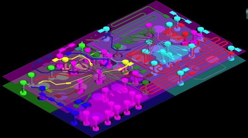
Image An example photonic SIP design in the Virtuoso environment
Although electrical simulation using the PCB and packaging-oriented Sigrity tools was already available, the integration is now tighter, Shay claimed. “You can select a trace and you can create an S-parameter model that will be embedded in the schematic. It will create the end ports and make the inter-port connections. You don’t need to do it yourself.”
To cope with more advanced processes, including the 5nm generation now in development at the foundries, Cadence has implemented what it calls simulation-drive flow to reduce the impact of electromigration and other parasitic effects. This builds on top of the existing electrically aware flow that has been used in Virtuoso for a number of years. The routing engine uses simulations of electrical effects to guide design.
“The system can compute on a channel basis where it has more or less current density and will automatically size the wires up or down so that it is correct by construction,” Shay said. “The layout topologies will be more appropriate for the EM challenges of the design.”
One of the major issues with mixed-signal design in sub-28nm nodes is the complex interactions of design rules and the need to cater for dummy structures to maintain yield. The company has used feedback from its IP-design team to inform its development of the layout-assistance features for the nanometer-geometry processes. “They see anything that’s happening in these advanced nodes,” Shay claimed.
Virtuoso uses a series of grids at different granularities, coupled with P-cells to place preformed multi-fin transistors at legal locations. The use of gridded layout makes it possible to deposit and move cells without using manual measurements to ensure design-rule compliance. As the cells are assembled they form part of a row-level grid that aligns with dummy cells needed to maintain the required fill density. The tool also uses the gridded approach to take care of end-of-line design rules.
At the routing level, the grids are automatically colored to ensure traces are placed on the appropriate multiple-patterning mask.