European teams explore 3D integration tradeoffs
Two leading European research institutes presented their work on the feasibility and cost-effectiveness of monolithic 3D integration at this year’s IEDM. Both show the emerging trend towards sequential integration in which layers of different types of circuitry are built up on a single initial wafer.
In their work on power-performance-area-cost (PPAC) analysis, researchers at Imec found the best value from the use of a heterogeneous sequential-3D integration approach. This is one based on the separation of non-scalable analog and I/O from the more logic and memory scalable portions of the system.
What Imec calls sequential-3D integration (S3D) the vertical integration of sequentially processed device layers with isolation and interconnect layers in between. S3D then subdivides according to the granularity of the interconnect between the layers. This could be at the transistor level (T-S3D), cell level (C-S3D) or IP block level, known as heterogeneous S3D (H-S3D). All involve tighter integration than is available using stacked-die and through-silicon vias (TSVs).
According to CEA-Leti’s CoolCube research team, layer-by-layer buildup based on a mature 65nm BEOL process flow can achieve interconnect densities of more than 200,000 per square millimeter – more than an order of magnitude higher than the state of the art using TSVs to convey signals between multiple die in a stack.
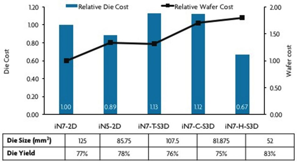
Image Die cost for three different S3D variations - T-S3D, C-S3D and H-S3D - versus 7nm and 5nm 2D versions.
Imec found the largest PPAC benefit was found for a H-S3D use-case. In this situation, the logic and memory part was scaled to iN7, Imec’s definition of a 7nm technology, with the analog and I/O IP moved to a layer that uses N28 technology in the top tier. For this use-case, despite a high wafer cost, a die cost reduction of 33 percent was achieved with respect to a 2D-SoC implementation with 125mm2 die size.
Leti’s work on 3D sequential integration indicates the choice of architecture and stacking process depends heavily on the target application. Integration of conventional CMOS-based systems with intermediate connections based on BEOL processes to achieve low delay comes with stringent limits on how much heat can be used to create the upper layers. Temperatures need to be kept to around 500°C, which could cause problems for performance on the transistors above the base layer. Leti argues the components for this have been demonstrated successfully but IoT applications could relax the requirements.
According to Leti, the development of neuromorphic computing architectures could promote the use of lower-performance transistors that are made using much lower thermal budgets than CMOS devices. Thin-film transistors and junctionless devices could support the lower clock speeds of energy-constrained IoT edge nodes. These can be made using sub-400°C processes, including the annealing steps that often require higher thermal budgets in CMOS. Analog devices fabricated with relaxed nodes should also have acceptable thermal budget stability, the Leti team argues.