Vertical structures to debut at IEDM 2015
A novel approach to 3D NAND will be among the presentations at the International Electron Device Meeting (IEDM) to be held in Washington, DC in December 2015.
Instead of opting for a gate all-around (GAA) architecture for a 3D NAND string, Macronix will propose the creation of a structure that is more like that of a traditional 2D NAND but tipped on its side to save on die space. The problem with current GAA NANDs is that they suffer excessively from tiny variations in critical dimensions – and these are difficult to control in the deep trenches used to hold the strings.
The Macronix SGVC structure is a single-gate, flat-cell thin-film transistor with an ultra thin body. The company claims it could ultimately offer four times the density of GAA structures at the same basic process node.
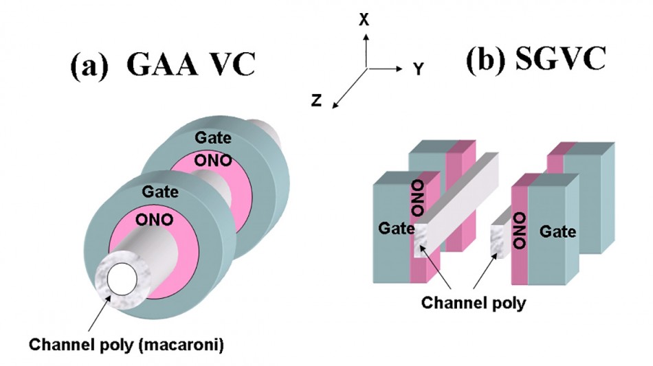
Image Comparison between GAA and Macronix's 3D flash structure (right)
In another session, researchers from the Taiwan National Tsing-Hua University will describe a resistive memory (RRAM) combined with a finFET for the select gate, with the transistor’s hafnium dioxide dielectric film used as the RRAM’s storage node. The architecture results in a cell area of 0.07632µm2 on a 16nm process with no additional mask or process steps.
Although flash memory designers are looking for alternatives to the GAA architecture, the structure is one possibility for future nanowire transistors. A team led by Taiwan’s National Nano Device Laboratories will describe how they built GAA nanowire MOSFETs with diamond-shaped Ge and GeSi nanowire channels, using the odd shape to exploit the properties of different facets of the crystal.
The purpose of the work was to find a way to more effectively use germanium as the channel material in multi-gate device configurations, because the high mobility of germanium is seen as potentially necessary for scaling beyond the 10nm technology node.
Using common dry etching and blanket epitaxy techniques, the researchers sculpted Ge and GeSi nanowires into diamond cross-sectional shapes, with four favorable facets – employing the {111} orientation – exposed.
For an experiment intended to align nanowire technology with CMOS, a team led by National University of Singapore will describe a use of vertically stacked III-V nanowires. Using a thin, sub-150nm high-quality gallium antimonide (GaSb) buffer layer on silicon. On top of it, the researchers built multi-gate indium arsenide (InAs) nFETs and GaSb pFETs from stacked InAs or GaSb nanowires, respectively.
Although the subthreshold slope remains high, the researchers are reporting a slope of 126mV/decade and drain-induced barrier lowering of 285mV/V for the InAs nFET with a 20nm channel length. The lowest reported subthreshold slope so far at 188mV/decade and the highest reported Ion/Ioff ratio of 3.5 were demonstrated for the GaSb pFET, which had a channel length of 500nm.
The 2015 IEDM will take place at the Washington DC Hilton Hotel from December 7-9, 2015, preceded by day-long short courses on Sunday, December 6 and a program of 90-minute tutorials on Saturday, December 5. In addition to a technical program of some 220 papers, a number of other events will take place during the meeting, including evening panels, special focus sessions, IEEE awards, and an entrepreneurial luncheon sponsored by IEDM and IEEE Women in Engineering.