Cadence updates Virtuoso for the 20nm generation
Cadence Design Systems has built into its latest update for the Virtuoso custom-design environment a number of features designed to tackle the problems of working with the 20nm generation of processes, with some pointers on what to expect as finFETs head into production at the pure-play foundries. Color-aware layout for double patterning, features to handle a new class of local interconnect and a more iterative approach to mixed-signal design are among the changes.
Steven Lewis, product marketing director for the custom-design tools at Cadence, reckons this is the third inflexion point in hand-tuned design in a decade. “We have found with customers that there were inflexion points over time. One was at 90nm. From there many found they could go relatively easily to 65nm or 45nm and many simply leapt over 90nm and landed on 65nm or 45nm. We found those techniques lasted until 28nm and then new design rules came in, making it another inflexion point. Now we are finding that there is an even larger one at 20nm. And preliminary work at 14nm and 16nm has found things designers will need to be aware of there.”
Lewis said there are three main issues the latest update tackles: “The first is layout-dependent analysis. The schematic is not the design anymore. Much of the way the circuits work is down to how they are laid out and routed. There was a time when designers set circuit and device parameters and then sent those to a layout designer. That over the wall approach isn’t going to work anymore.”
The changes in stress depending on how close a transistor is to something like a well boundary leads to big changes in properties such as threshold voltage. “To figure out these layout-dependent effects you need to go to layout as quickly as possible,” Lewis said. “The layout really is the design now.”
One possibility is to automatically synthesize a number of candidate designs, have them laid out and pick the one that works. “We don’t find a lot of value in that. If you have to rip choices they give you, why did you bother? With us, it’s check as you go,” Lewis argued.
“We allow the designer now to do a partial layout and then simulate. You can take advantage of MODGENs and place those down or just a single transistor. And then analyse what is going on. Traditionally the LVS tools and extraction tools have relied on having a complete design. But, with this you don’t have to be LVS or DRC clean. You can go ahead, put down transistors and calculate their layout dependent effects.”
If the design is not likely to meet its objectives, the placement and routing can be changed. If it is, then more of the rest of the circuit can be placed, simulated and assessed. “We fill in whatever is missing via the schematic. The new BSIM models that people now use for planar transistors are already characterised for nominal values of layout-dependent effects. So, the transistor model that comes from the foundry can be used as a substitute for any cells you haven’t laid out yet,” Lewis explained.
The second issue surrounds double patterning and provides designers with the ability to assign critical elements – such as matched elements – to individual masks and have the tool re-color the rest of the layout to suit – just as long as putting the new shapes down does not lead to an impasse because two elements of the same color wind up too close to each other.
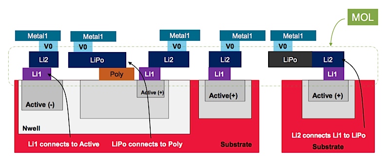
Figure 1 The latest version of Virtuoso adds support for new types of local interconnect proposed by IBM and other foundries
The third change is around the new form of local interconnect that is springing up on 20nm processes. IBM revealed at the VLSI Technology Symposium last year how it aims to use via-free local-interconnect layers – or rather vias that have been fractured into sublayers so that they do not have to be purely vertical – to provide dense routing between the poly and proper metal-one layers. Other foundries appear to be adopting similar techniques, which need special treatment from layout tools and routers.
“These layers are very specialized and there are very specific rules in how you go from one layer to another,” said Lewis.
For the latest update, Cadence has added support for finFETs but is looking at ways to represent them in designs to make them easier to work with. “We think the best way going forward is to use MODGENs, but it remains to be seen,” said Lewis.