DATE: The real causes of carbon nanotube FET performance variation
The performance of carbon nanotube FETs is more affected by the way that the nanotubes are grown and deposited than by the traditional sources of variation in silicon-based devices, according to the team that unveiled the first CNFET subsystem earlier this year. At DATE, it also detailed design strategies for overcoming them.
The Stanford University group, which presented a CNFET sensor interface at ISSCC, said that it encountered far more issues from CNT-specific variation than from factors such as channel length, oxide thickness and threshold voltage.
These CNT-specific variations can degrade the technology’s speed benefits by up to 60% at the 16nm technology node.
The most important sources of CNT-based variations were:
- Variations in the density of grown CNT, caused by non-uniform spacing between CNTs on the substrate.
- Variations caused in the number of semiconducting-CNTs that remain after the use of processes to remove metallic-CNTs.
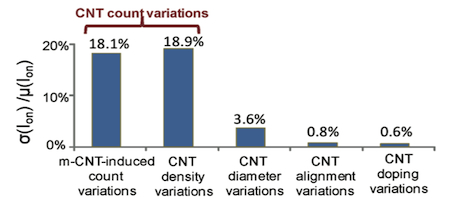
- Figure 1. Relative contributions of CNT-specific variations to CNFET on-current variations (Source: Stanford University)
The debate surrounding CNT-specific variations has focused on the impact of the diameter of CNTs in single CNT devices, although this may be because of the nature of pathfinder projects.
“The On-current of a CNFET containing only a single CNT is quite sensitive to CNT diameter variations, … CNFETs in practical circuits require multiple CNTs in order to achieve high On-current values. Due to statistical averaging, such CNFETs are not very sensitive to variations in diameter, alignment, and doping,” Stanford says in its DATE paper.
The team is trying to overcome the CNT-specific variations by making the tubes’ diameter bigger. Using this technique on its own surrenders many of the potential low-power benefits of CNFETs. These can be regained using, among other ‘knobs’, a novel co-optimized design/process strategy.
Stanford has developed what it calls ‘aligned-active’ layout, which lines up the active regions of all the CNFETs in a design.
“CNFETs whose active regions are aligned along the CNT direction share the same set of CNTs, and therefore have highly correlated CNT counts,” Stamford’s paper explains.
“If the CNT counts of multiple CNFETs are correlated, then so are their individual probabilities of CNT count failure. As a result, the probability that at least one of these CNFETs has CNT count failure decreases. Therefore, engineering more CNT count correlation between CNFETs can improve count-limited yield along the direction of the aligned CNTs.”
In itself, ‘aligned-active’ layout reduces the probability of a CNT count failure by more than an order of magnitude. This can then be further tuned by the use of processing enhancement techniques, co-optimized with the alignment.
The work still places CNFETs some way from commercial use – though this is not expected until single-figure nanometre nodes anyway. The Stanford researchers acknowledge that further work on both co-optimization and ‘imperfection-immune’ design (to overcome the presence of m-FETs) will be needed.
