Putting chiplet design on the ‘smart path’
Chiplets answer the difficulty designing monolithic ICs for advanced nodes but they present their own challenges for areas such as floorplanning and optimizing PPA. Consequently, packaging is a delicate task.
An extended technical article – originally published in IMAPS Advancing Microelectronics Magazine – Device Packaging – describes a flow based on homogeneous disaggregation that counters some of the inherent complexity. It is described through the example of a 4 HBM silicon interposer technology.
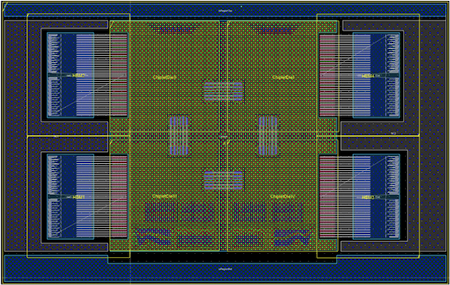
Figure 1. The top level 4-HBM_chiplet example showing the chiplet and HBM die-to-die interfaces (Siemens EDA)
The example is comprised entirely of parametric pin regions. This reflects the mushrooming in pin count common to packaging design for chiplet-led projects.
‘The smart path to chiplets using hierarchical device planning and pin regions‘ leverages a collaboration between Siemens EDA and Intel Foundry Services.
The detailed paper organizes its description of the technique across the following topics:
- Introduction from Intel Foundry Services
- The path to chiplet architectures
- Floorplanning environment
- Die-to-die building blocks
- Arrayed building blocks
- Power distribution networks
- Parameterized pin regions
- Homogeneous disaggregation of SoC
- Conclusion
- References
“While it may still be possible to generate an initial draft of an advanced IC package design using nongraphical IC package floor-planning flows, it simply would not be feasible to keep up with the changes required by early design analysis,” writes author Chris Cone.
“With an HBM die-to-die building block in place and using parameterized pin regions, package designs… can be created quickly and efficiently.
“More significantly, iterative updates can be done in a matter of minutes or in some cases seconds because of effective incorporation of hierarchy in the design.”