Cadence pulls Virtuoso and Allegro closer for 3DIC
Cadence Design Systems has brought its chip- and PCB-design environments closer together as the shift towards multichip packages gains pace.
Cadence has made it possible to bring electrical models generated by its Sigrity board- and package-level signal-integrity analysis tools into the Virtuoso environment. The company has also automated to a much greater extent the job of performing layout-versus-schematic (LVS) checks across all of the devices that need to be incorporated into a 3DIC or system-in-package (SIP) design.
John Park, IC-packaging product-management director at Cadence, said: “Putting everything onto a single SoC can become expensive now. If you are shipping in high volume you can recoup those costs. If you are designing lower-volume systems it’s impossible to recoup those costs. Also, analog and RF don’t take advantage of Moore’s Law scaling.”
“Historically, heterogeneous integration has been driven by the systems companies where form factor is an important part of the equation. Now, there is a lot more interest in heterogeneous integration coming from the traditional semiconductor companies. They are looking to alternatives to just following Moore’s Law,” Park added, noting that a further trend is to take the idea of heterogeneous integration to the IP level rather than integrating functional die.
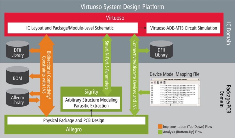
Image Data flows in the Virtuoso-Allegro-Sigrity integration
The move to adopt heterogeneous integration by chipmakers is seeing them begin to break apart SoCs and move IP off-chip where it makes sense to use a different process or to make it easier to mix and match functions. “They are essentially manufactured blocks of IP that let you do this Lego-like assembly,” Park said.
To design SIPs as groupings of IP calls for a move away from design silos, where packaging and board-level design takes over once the core SoC is complete. There needs to be more communication between electrical analysis at the board and package level and IC design, Park noted.
Sigrity is used to perform an electrical analysis supported by the process design kit (PDK) provided by the foundry or OSAT provider. The models the tools creates of offchip interconnects can be brought back into Virtuoso for use in PSpice or Spectre simulations that incorporate all of the devices in the SIP. Support for LVS across the Virtuoso DFII database and those used by Allegro helps keep the design consistent across the different environments automatically. The flow of LVS data between Virtuoso helps support the mapping of the Sigrity-generated electrical data into the cell instances used in Virtuoso’s schematic view.
“This is about concurrently designing packaging while designing the chips that go inside. If a user wants to take, say, a bandpass filter off the chip and move it onto another one inside the chip, they will be concerned about the interfaces between the IP that are now laid out in two different domains. This allows them to simulate how that filter behaves in their interconnect structure,” Park said.