X-Fab aims at lower-cost SiC with upgraded 6in line
X-Fab Silicon Foundries has upgraded its 6in fab in Lubbock, Texas to handle silicon carbide wafers in parallel with existing silicon production in an attempt to improve the economies of scale for power devices based on the wide-bandgap material.
The company has installed equipment to let it manufacture vertical diodes and transistors using silicon carbide wafers, including the specialist backgrinding tools needed to thin wafers made from a material that is almost as hard as diamond.
Andy Wilson, director of strategic business development, said the plan to incorporate silicon carbide into the production flow would help deal with an anticipate a migration of the fab’s existing automotive business to more advanced silicon-based processes.
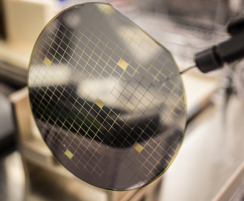
Image A silicon carbide wafer processed at X-Fab
Equipment reuse
“We wanted something that could utilize the existing equipment set as much as possible. That led us to silicon carbide. We saw that silicon carbide is making the transition to 6in [from 4in and below]. It’s at the very front-end of that production cycle,” Wilson explained.
“There are some speciality processing requirements but much of the existing equipment set could be converted to process both silicon carbide and silicon. Silicon carbide provided a really good fit within our existing foundry strategy,” Wilson added.
The ability to run an emerging process side-by-side with more established production flows should help deliver economies of scale more rapidly, Wilson claimed.
“If you are only running a small number of wafers through a line, that small amount has to absorb the whole overhead. The fundamental model we have put in place by embedding the line in an existing silicon line is that the majority of the overhead that’s required is supported by a silicon line that is still in high-volume production. We don’t have to burden the silicon carbide production and we can pass on the economies of scale on. If we can jump start the economies of scale, that will start to reduce the price premium that currently exists between silicon carbide and silicon and, in turn, accelerate adoption of silicon carbide.”
Switching migration
Although as a foundry, the types of device being run will depend on demand from fabless customers, X-Fab expects much of the initial work to focus on diodes. Often copackaged with silicon power transistors, silicon carbide diodes have already been commonplace in high-voltage switching. “Diodes represent the largest revenue stream for silicon carbide today,” said Wilson. “Longer term we are really excited about the viability of the switching market, starting in the 650V to 1200V range and then, eventually, going higher to 3.3kV where you can utilize the advanced capabilities of silicon carbide to support lower switching losses and increase switching speeds.”
Wilson said the existing support for long-lifetime products and automotive quality standards mean processes are already in place to support other markets, such as industrial power, that have similar requirements. Longer-term, automotive users may also start to move to silicon carbide because of its ability to survive the high temperatures encountered inside the engine. This may drive the development of planar processes optimized more for sensors than high power.
“It may be a few years past 2020 before we see significant volumes coming out of automotive,” Wilson said.
Backside processing
Wilson said the foundry is working with customers on techniques for backgrinding and thinning wafers, aiming to get down to the 180µm range in terms of wafer thickness to help reduce on-resistance in vertical power devices. Along with other high-temperature processing kit, laser annealing equipment brought in for the upgrade will support the ability to form ohmic contacts on the backside of wafers after thinning without subjecting the topside to the damaging high temperatures of bulk annealing processes.
The upgrade of the fab to handle silicon carbide was helped by support from the Power America Institute based at North Carolina State University, which has the role of encouraging research in wide-bandgap devices and processes. “It brought in matching funding that really allowed us to accelerate our investments,” Wilson said. “The support that we received from the Power America Institute has been the driving force and pulled us several years ahead of where we might have been otherwise.”