Achieving the interactive development of low-power designs
It’s obvious that many chip designers care about power consumption. Clearly, any product that runs on batteries for the majority of the time should operate at the minimal power necessary to perform its function in order to prolong operation while unplugged. This is a major challenge for complex handheld devices such as tablets and smartphones. Power is also a factor for many classes of Internet-of-things (IoT) device that may be in locations hard to access.
However, in recent years power has become a consideration for even the largest electronic products. Today’s server farms cost more in electricity over time than the initial cost of the hardware itself. It is impractical to locate every server farm adjacent to a hydroelectric dam or massive solar array. Reducing power must be part of any attempt to lower operating costs. In some locations, environmental laws place restrictions on power consumption from the electrical grid, increasing the need to design with power in mind.
The result is that most, if not all, contemporary system-on-chip (SoC) devices use low-power design techniques. These range from circuit-level tricks to software-controlled systems that track applications running in the SoC and adjust power to the minimal level. Most of the common techniques rely on being able to control different parts of the chip independently. The design is divided into power domains, each of which can be powered down when idle and powered up when needed to perform a particular task.
As an example, an external interface with nothing connected likely can be turned off. If the currently running applications do not require floating-point computations, the FPU can be put into sleep mode. Some power domains may offer finer-grained control, such as variable operating voltages or clock speeds to raise and lower power consumption without turning on and off completely. The process of understanding low-power needs and defining power domains starts during the architectural phase and continues throughout design and verification of the SoC.
Specifying power intent
It is not unusual for SoCs to contain dozens, or even hundreds, of power domains, not all of which are truly independent. Only certain combinations of domains turned on and off make sense, and each such combination is commonly called a power mode. For example, a chip with 50 power domains may have only 100 power modes defined rather than the more than one quadrillion (250) combinations theoretically possible. If some of the power domains can run at multiple voltages, then more power modes may be defined.
The rules for power modes and the transitions among them can be complex, as are the power controllers that scale the power domains up and down. Understanding these rules, designing the low-power logic correctly, and verifying the design are all significant challenges. The consequences of a bug can be severe; there are scary tales of fabricated chips with a power domain that cannot be turned back on once it has been powered down. This can lock up the SoC and require a costly respin to fix. Some chips are designed so that not all power domains can be on at the same time; if this happens due to a design bug the result can be thermal runaway and permanent damage.
For all these reasons, low-power development teams sought a way to define power intent in an unambiguous way that could be shared among all teams across the development flow. Two industry initiatives to address this need arose in the 2006-2007 timeframe. Accellera created the Unified Power Format (UPF) while, roughly in parallel, the Silicon Integration Initiative (Si2) defined the Common Power Format (CPF). UPF was standardized as IEEE Std. 1801-2009 and later revised to IEEE Std. 1801-2015. This included some features from CPF, which now has a version 2.0 released.
One critical decision made for both formats was that the power intent is specified in a separate file, distinct from the design file. This allows power intent to be specified early in a project and that specification can span from SystemC architectural models through RTL code to gate-level netlists. This would clearly be harder to do if the power intent were, for example, captured by pragmas in the RTL. A separate file also allows easier sharing of power intent between related projects. Separation of design intent and implementation is generally considered good engineering practice.
The downside of this approach is that it is common for the RTL implementation and the UPF or CPF file to fall out of synchronization as the design evolves. Especially if the power intent is defined early in the project, changes are highly likely. Implementation details may change, the design hierarchy may evolve, and signals may be renamed in the RTL. In parallel, changes may be made to power intent in response to new features, competitive pressure, or estimation of power consumption. Keeping the two files aligned can be an ongoing challenge.
An IDE solution
Fortunately, the well-established concept of the integrated development environment (IDE) can be expanded to develop RTL and power intent files in parallel, keeping them in lockstep as both evolve over the course of a project. Engineers can develop, test, and debug their code interactively. IDEs are available to support the full range of software programming languages, modeling languages, hardware description, and dedicated verification languages, including both the design and verification features of SystemVerilog. An IDE can:
- Perform many types of checks on the code;
- Highlight and format the code according to user preferences;
- Compile the code to present the complete design and testbench structure;
- Connect to a simulator for debugging failing verification test cases; and
- Provide an intuitive graphical user interface (GUI) for code development.
Adding IDE support for UPF and CPF is a natural and high value next step for low-power design. Because the IDE compiles the power intent files along with all the design and verification source code, it can build an internal database of the complete environment. The knowledge encapsulated in the database enables sophisticated operations such as traversing deep design hierarchies, finding a wide variety of coding errors, making suggestions for fixes, and autocompleting and providing templates for new code. The IDE can even perform refactoring operations that make the code more readable, more maintainable, and better suited for later project steps such as simulation and logic synthesis.
Synchronized development of low-power designs
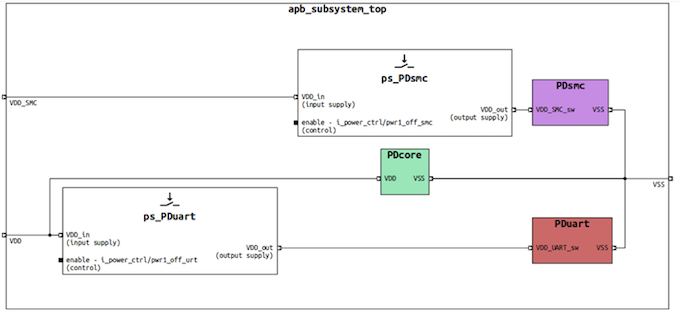
One of the key benefits of the IDE is its ability to present multiple views of the design and verification environment code. These views include code editors, block diagrams, schematics, and hierarchy browsers. In the case of UPF or CPF, the primary view is the supply-network diagram. It shows all the power domains and power switches, and how they are connected by power supply nets and ports. Figure 1 shows the supply network diagram for a portion of a chip containing three power domains and two voltage sources. This screenshot and the others that appear in the following examples are from the Design and Verification Tools (DVT) Eclipse IDE from AMIQ EDA.
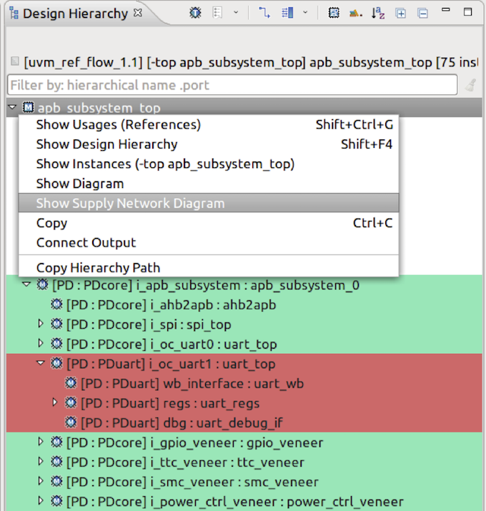
Two of the power domains have the ability to be shut down by power switches under the control of enable signals, as specified in the power domain file. Color coding is used to clearly differentiate the power domains and to provide an easy way to cross-correlate across the different views provided in the IDE. Figure 2 shows a design hierarchy view that not only shows which parts of the design lie within which power domain, but also colors the domains to match the colors used in the supply network diagram.
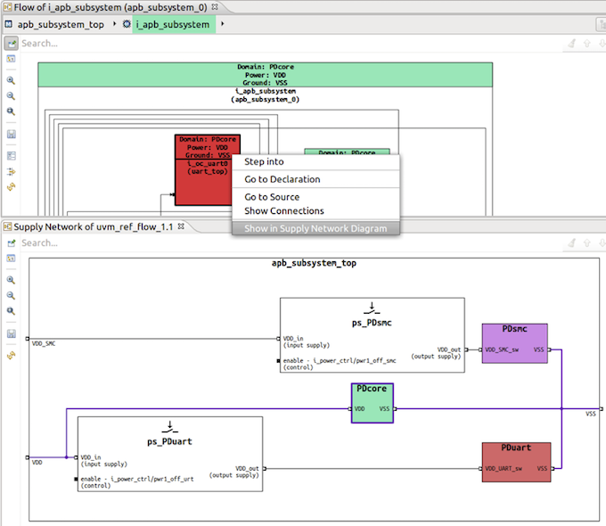
Figure 2 also shows how users can generate the supply network diagram from the design hierarchy. The IDE makes this sort of navigation among its different views natural. For example, it is easy to select a particular power domain and display its connections. Figure 3 shows a flow diagram view in which the user has highlighted the ‘PDcore’ power domain and specified that it should be shown in the supply network diagram. This produces the same diagram as in Figure 1 except that the selected power domain and all its supply nets are highlighted.
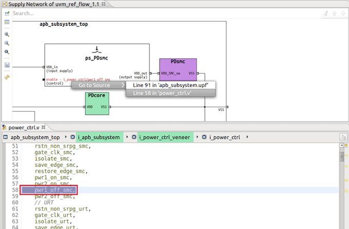
It is also possible to navigate from the supply network diagram to other views easily via the IDE’s cross-referencing capabilities. Figure 4 shows the user highlighting one of the power control signals and selecting to view the RTL source file that contains the signal. The IDE brings up a code editor view, jumps to the line where the signal is defined, and highlights it. As the pulldown menu shows, the user can also choose to bring up the power intent file and show where the signal appears in that description.
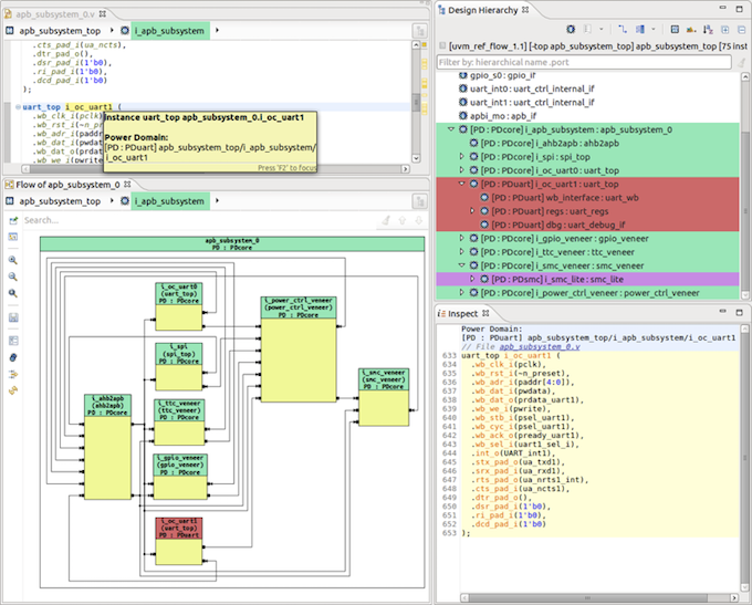
The combination of these views provides a comprehensive look at a low-power design. Figure 5 shows a UART instance selected from the RTL code. The inspect view gives more details and context for the instance; the design hierarchy view jumps to the instance; and the flow diagram view displays the instance and identifies its power domain. The configuration of views is entirely up to the user. Other views that could be shown include the UPF/CPF source and the supply network diagram.
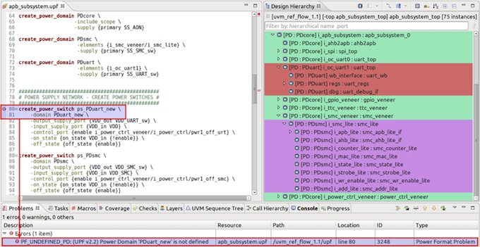
The IDE provides support for numerous design and verification languages, including SystemVerilog, Verilog, VHDL, e, and C/C++. The many features of the IDE for these languages are also available for CPF and UPF files. These include detection of errors, auto-correct, auto-complete, and suggestions. Figure 6 shows an example of an error in which a power switch references a power domain that has not been defined. The IDE detects the error, reports it, and highlights the location in the power intent file.
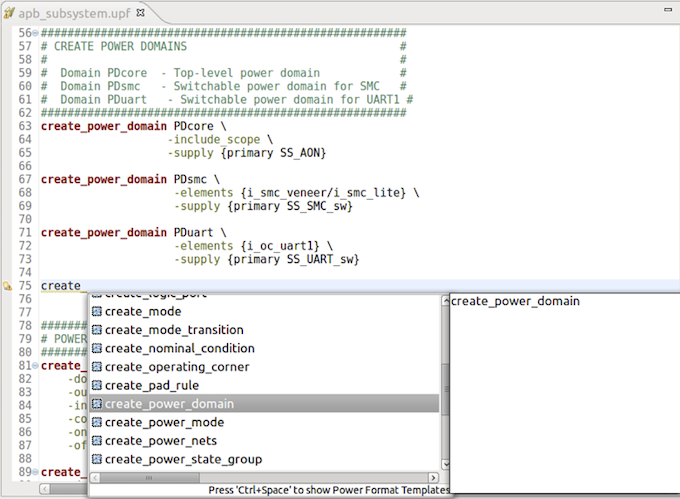
Auto-correct and auto-complete capabilities accelerate the process of creating and refining power specifications. If an engineer makes a mistake, such as typing ‘create_power_domains’ into the UPF editor, the IDE instantly reports this as an error and recommends a correction to the proper ‘create_power_domain’ command. As shown in Figure 7, if the user types in only ‘create_’ the IDE pops up a menu showing the possible completions and allowing the user to choose the intended command.
Any time an edit is made to a design file or power intent file, the IDE re-compiles the changed file, updates its internal database, refreshes all views, and reports any inconsistencies. This enables the development team to keep RTL and power intent synchronized throughout the project despite the inevitable evolution of the design.
Conclusion
Low-power chip design is nearly ubiquitous today; several factors drive development teams to minimize power consumption as much as possible. The introduction of power intent files was a major upgrade to low-power design and verification, providing a single description to be shared across project teams and used by EDA tools to automate some steps of the development process. However, renaming and other changes in the design can quickly and repeatedly render the power intent file outdated. The visualization, cross-referencing, and cross-checking nature of an IDE provide an excellent solution. This makes it much easier for design and verification engineers to create, manage, and validate power domains, from IP blocks all the way up to large SoCs, and from the architectural phase to tape-out. The IDE is essential in the low-power design toolkit.
Further reading
This article is the sixth in a 12-part series providing a comprehensive and detailed analysis of the value and deployment of IDEs. You can access all the other parts by following the links below, presented in order of publication. You can also learn more about the Eclipse IDE from AMIQ EDA by following this link.
- Why hyperlinks are essential for HDL debugging
- A helping hand for design and verification
- Correct design and verification coding errors as you type
- Take advantage of the automated refactoring of design and verification code
- Delivering on the advanced refactoring of design and verification code
- Achieving the interactive development of low-power designs
- Accelerating the adoption of portable stimulus
- Accelerate your UVM adoption and usage with an IDE
- VHDL users also deserve efficient design and verification
- How IDEs enable the ‘shift left’ for VHDL
- Extract benefit from the automated refactoring of VHDL code
- e language users deserve IDE support too
 Tom Anderson is a technical marketing consultant working with multiple EDA vendors, including Agnisys. His previous roles have included vice president of marketing at Breker Verification Systems, vice president of applications engineering at 0-In Design Automation, vice president of engineering at IP pioneer Virtual Chips, group director of product management at Cadence, and director of technical marketing at Synopsys.