Plasmonics may point way to faster interchip comms
The energy consumed per bit in chip-chip transfers continues to be a limiting factor on the performance of package- and PCB-level integration. Silicon photonics is one possibility but it remains a bulky option. A group at the University of Toronto working with Arm believes moving to plasmonic techniques could overcome those limitations.
Plasmonics, which uses interactions between electrons and photons to control light, has typically shown worse performance than silicon photonics at the kinds of speeds that would make either attractive as alternatives to existing inter-chip communications schemes. But in principle, plasmonics could offer better integration because it does not suffer from the same diffraction limits on device size or the need for thermal control, which has a knock-on effect on latency as well as cost.
In a presentation at IEDM last week University of Toronto postdoctoral researcher Charles Lin pointed out a problem with conventional plasmonic structures: “The challenge is that many existing designs still use non-CMOS compatible metals and suffer from insertion losses that can be as high as 10 to 20dB. This is because, while metal enables much stronger light confinement, it also acts as a light-absorbing medium. There is a trade off between loss and confinement in existing plasmonic waveguide structures.”
The way around this tradeoff is to move to a silicon-based waveguide structure, which the team has called coupled hybrid plasmonic waveguide (CHPW). This places a Schottky junction on top of a MOS semiconductor sandwich with a thin aluminium layer between them. The asymmetric structure gives rise to interference modes that changes the loss-confinement tradeoff. “This interference is very effective for loss reduction,” Lin claimed. “The interference can allow you to have almost independent control of loss and confinement.”
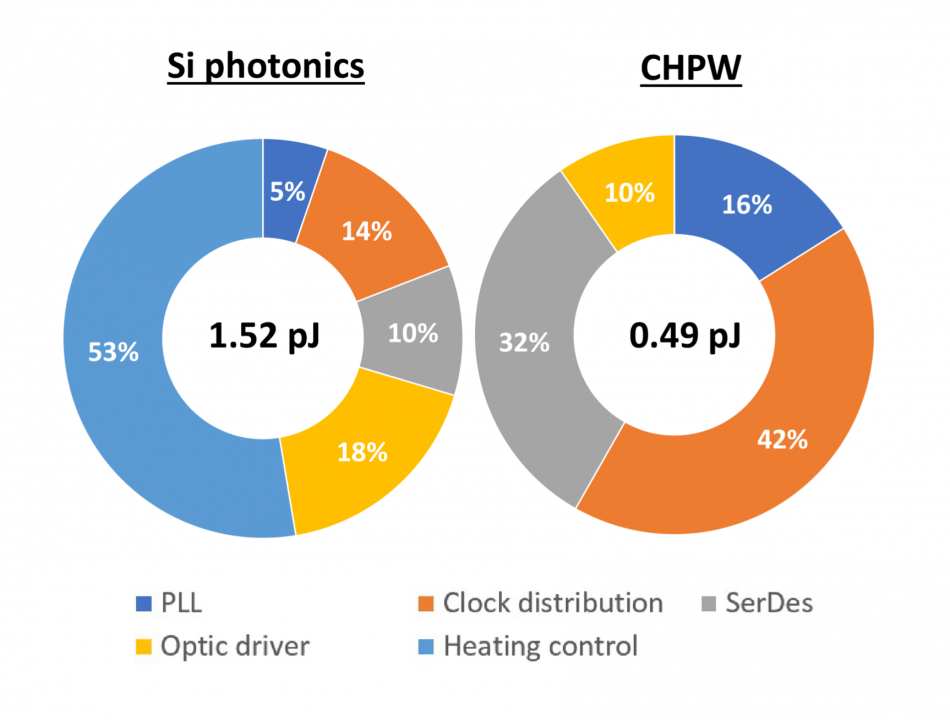
Image Energy contributors for photonic and plasmonic waveguides
A second advantage, according to Lin, is that subtle changes to device dimensions can tune the CHPW for different applications. For example, altering the width changes the performance from a low-loss passive element to an efficient photodetector. “The devices can be integrated very close together, which can reduce the cost of integration significantly,” Lin said.
A numerical study of expected performance based on the devices made in the university’s lab indicated that while silicon photonics would likely top out at just under 40Gb/s over a distance of 1m in fiber without bit-error correction in an Ethernet-type application, plasmonic modulators and photodetectors could push the datarate to 150Gb/s. “We expect that could be better if made using standard foundry processes,” Lin claimed. “We project plasmonics can approach a density of 100 terabit per second per meter squared.”
In comparison, silicon photonics looks to have a bandwidth density of around 1.5Tb/s/m2, with about three times the energy per bit and much higher latency because of the need for thermal stabilization.
The group is now working on intra-package waveguide systems as the researchers believe the technology could suit a range of system-level interconnect needs from system-in-package to board-to-board.