Backside metal defends against IR drop and side-channel attacks
When Imec proposed the possibility of capitalizing on buried power rails and pushing the power distribution network to the die’s backside in future generations of CMOS, the main attraction seemed to be denser logic interconnect on the frontside. But work by a team based at several universities in Japan shows taking advantage of the backside surface for power and ground can deliver further benefits for IR drop and security, especially when combined with 3DIC stacking.
In his talk at IEDM this week, Kazuki Monta, one of the researchers on the team and who is based at Kobe University, noted that Imec had proposed the use of backside metal in logic-oriented chips for integrated inductors. This work focused more on distributing capacitors through a stack of ICs to help deliver more reliable power.
The test vehicle for the experiment was a cryptographic controller accompanied by a onchip voltage regulator module. To ease implementation for these tests, the same chip was used in all the layers of a four-tier 3DIC stack. Through-silicon vias linked the power grid to onchip logic and I/O, with microbumps used to connect the layers and the stack to the PCB-level package. Rather than use metal-in-metal (MIM) capacitors, the team opted turn the supply rails into several meshes, forming distributed capacitors between the metal and the silicon substrate. Ground and I/O connections were made in strips of pads in between the Vdd meshes. The overall deliverable capacitance is smaller than with MIM passives, or metal-on-metal, but does not sacrifice as much die area to them.
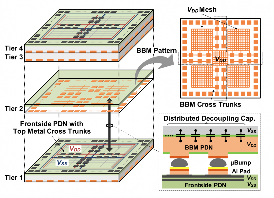
Image The structure of the IC stack using backside metal and supply meshes
The resulting combination of distributed capacitance and onchip regulation saw IR drop by around 60 percent and series impedance by just over 40 percent, Monta claimed. A further benefit turned out to be improved immunity to side-channel analysis: a hacking technique that gleans information from EMI emissions and which makes it possible to find secret key bits if enough traces can be collected by an attacker.
In the case of the chip stack, as the ICs are mounted upside-down, the top of the stack can be used as an EM shield, which significantly increases the number of traces an attacker has to record to be able to crack keys. However, the effectiveness is around the same as a dedicated shield on a conventional cryptoprocessor, they found. However, the lower susceptibility to IR drop resulted in dramatic improvements in tests based on probing on the power rails, compared to conventional shielding techniques.
The work by Monta and colleagues has some similarities in approach to that of work presented earlier this year at the Custom Integrated Circuits Conference (CICC) by Purdue University, Georgia Institute of Technology and Intel that promises to be highly resistant even to side-channel analysis that exploits machine learning to tease more hidden correlations out of the emissions data. In that work, the cryptoprocessor was decoupled from the main power grid and upper metal layers, which in turn were used as EMI shielding, by onchip power regulators. Those onchip power regulators are designed to inject noise into the power rails that can be probed by an adversary if they do not go to the extent of stripping the metal shield, an intrusive attack that might trigger active countermeasures in any case, such as a refusal to boot.