Five steps to faster FPGA implementation
How do you speed up the process of implementing complex designs in large FPGAs, given the increasing complexity of their architecture and the growing average design size?
A webinar produced by Synopsys walks viewers through five steps users of its Synplify Premier tool can take to ease the process of implementing a complex design on FPGAs from Altera and Xilinx.
1 – Set up your design flow
The first step is to make sure that your design flow has been correctly set up to enable automated synthesis using IP from both internal and third-party sources.
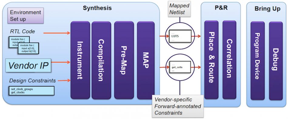
Figure 1 The basic design flow for complex FPGA implementations (Source: Synopsys)
An important part of this set-up process is gathering and, in some cases, generating IP blocks to include in the design. The webinar walks viewers through two processes for configuring and importing IP, which may have been delivered in a variety of formats offering differing levels of access to the IP, for Altera and Xilinx target devices.
In the ‘absorb’ approach, the entire IP is read in and then the synthesis engine can optimise the timing paths and logic around and within the IP, so that the final design netlist includes the IP netlist. The second approach treats the IP as a white or grey box> This means that the content of the IP can’t be optimised by the synthesis tool, which instead has to focus on optimising the critical timing paths around the IP block.
The webinar goes on to advise on which approach is most suitable for various forms of IP, and also details how to work with the FPGA vendors’ tools to have them generate their IP blocks in the format most suitable for use in Synplify Premier. It also covers issues such as checking that timing constraints are correctly passed from the vendor tools to Synplify Premier to help drive the synthesis process.
2 – Set up your constraints
Having set up the basic design flow, configured and generated the appropriate IP for inclusion in the overall design, the second major step is to set up the FPGA design constraints, and the clock and input constraints, to inform the synthesis and place and route processes. Writing the correct timing constraints involves identifying all the clock signals, creating clock groupings and relationships, constraining those clocks, and the inputs and outputs, and finally defining multi-cycle paths and false paths. The webinar details a couple of utilities that are available to ease the constraints development process: a template utility and a graphical user interface called SCOPE.
3 – Clean up your design
The third step covered in the webinar is ‘pipe cleaning the flow’, that is, finding ways to use it to make rapid progress in finding and fixing obvious bugs and issues, so that these don’t slow down the more time-consuming implementation stages later in the flow. The webinar discusses the use of ‘continue on error’ switches in the design compilation process, so that any bugs created when adding a new block to a design are noted and ignored – rather than stopping the compilation process in its tracks for each one. A fast synthesis mode can also be turned on to speed up early compilation runs by reducing the number of optimisations that are applied. Fast synthesis also creates a timing report that can guide the refinement of timing constraints.
This step also includes constraint-checking tools to verify both the syntax and validity of constraints before full synthesis. This process produces a report on issues such as clock relationships, unconstrained I/Os, start/end points, name collisions, misinterpretations, inapplicable constraints, and non-locked I/Os. It is also possible to verify forward-annotated constraints, that is FPGA design constraints that will be translated into vendor-specific formats and passed forward to vendor tools to drive place and route.
The webinar also discusses the use of distributed compilation and/or synthesis as part of this pipe-cleaning phase, as a way of accelerating these processes by sharing the task out over a large server farm. One of the advantages of this approach, along with speed, is that it means larger designs can be handled without being limited by the memory constraints of a single machine.
4 – Optimize performance
The fourth step covered in the webinar is optimising a design for maximum performance by applying advanced synthesis strategies, post place-and-route re-synthesis techniques, and exploratory place and route schemes. The webinar details how advanced synthesis can be used to address timing issues, the use of exploratory place and route techniques to automatically try out different ways of overcoming potential routability issues, and the use of post place-and-route re-synthesis strategies to address timing and routing issues by reducing routing congestion and critical-path delays.
5 – Bring up the design and debug it
The fifth step detailed in the webinar is bringing up the design. This focuses on some of the challenges of verifying the design, the unique aspects of verifying an FPGA-based implementation, and some of the tools available in the flow to instrument the FPGA to give visibility of internal signals at full system clock speed. There’s also a look at some basic debug strategies that can be implemented using this combination of hardware instrumentation instantiated in the design and external debug tools that can interact with it.
The webinar, presented by Paul Owens of the Synplify Business Group at Synopsys, is available on demand here.