Overcome IoT edge challenges with integrated flows
The design of IoT edge devices can appear as challenging as squaring the circle. These products are highly cost-sensitive, yet must incorporate and integrate multiple domains. Budget pressures also mean that they are typically developed by small project teams that nevertheless must have experience of multiple design tasks.
Consider this description of a basic IoT edge device. “It contains a sensor that interfaces to the Internet. The sensor signal is sent to an analog signal processing circuit in the form of an amplifier or low pass-filter. The outputs connects to an A/D converter to digitize the signal. That signal is sent to a microprocessor to process and analyze the data. The sensor telemetry is sent and control signals are received by a radio module that uses a standard protocol such as WiFi, Bluetooth or ZigBee. The data is relayed up to the Cloud through an Internet gateway.”(1)
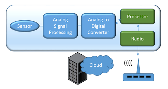
Figure 1. A typical IoT edge device (Mentor Graphics)
Easy enough to conceive, such a device still requires capabilities drawn from the digital, analog, RF and MEMS domains. Any sensor-based product must also function in various environments thereby also requiring some multi-physics analysis around factors such as temperature, vibration and pressure.
And remember all of the above must be achieved while keeping power consumption to the minimum.
Traditional design strategies fail this model. They are too expensive.
As noted, IoT edge designs tend to be highly cost-sensitive. One that extends the functionality of a large consumer product – a good example might be a drone – may have a little more room for maneuver but even there, it’s not much.
To find a better approach, we need to start by considering what a typical IoT edge design team needs to look like (and this model can as easily apply to a major company as an IoT startups).
The team will be small, and by ‘small’ you could well be looking at less than ‘one’ in terms of headcount for each of the major tasks (capture, simulation, layout, verification, etc) and/or the domains in which the device will operate.
The tools must therefore be ‘comfortably’ priced but at the same time easy enough to use so that they genuinely help team members working within and across multiple disciplines (silicon, embedded software, PCB). Given that, there should be relatively tight integration between all of those tools.
But at the same time, neither the nature of the team nor that of the tools should constrain the designers’ imaginations. Particularly for IoT edge products, developers need the freedom to explore various configurations and functional specifications.
An integrated IoT edge flow
Mentor Graphics has an offering that covers all the key stages in an IoT edge flow with tools specifically aimed at projects being realized on tighter budgets. Adopting such a flow from a single vendor also ensures the kind of thorough tool integration discussed earlier.
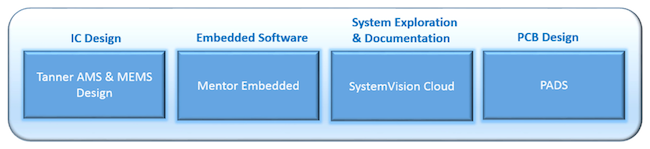
Figure 2. The integrated Mentor Graphics IoT edge flow
As shown in Figure 2, the flow offers IC design, simulation, layout and physical/circuit verification through tools marketed under the Tanner EDA name. Even before its acquisition by Mentor in 2015, Tanner had built a strong reputation at the bridge between silicon and MEMS, now so important for IoT edge projects.
Mentor’s long established Embedded division offers the Nucleus RTOS, specifically optimized for low-power projects, while its Sourcery CodeBench can be used to build, debug, analyze and optimize the software that will sit on top of that RTOS.
Mentor’s PCB offering, PADS, is a well-known, battle-hardened tool suite for tasks such as schematic capture and layout. It also recently underwent a major upgrade.
Finally, the SystemVision Cloud environment provides easy and quick access to an online environment for design exploration and the simulation of various ‘what if’ options.
The IoT edge is an exciting market. While there has been a greater ‘high margin’ focus on cloud or hub processing, it is worth noting that some analysts now predict that more than 90% of the big data gathered will need to be processed at the edge. Successful edge products will combine cost-conscious design with increasingly sophisticated functionality. Flow integration can help resolve obvious tensions here.
Further reading and notes
1. For a deeper look at how Mentor’s IoT edge flow has been constructed, read the whitepaper, Driving Intelligence to the IoT Edge Invents a New Breed of Designers, by Jeff Miller.