Tensilica vision processor cuts power through memory changes
Memory efficiency has driven the design of the latest video and image processor core developed by the Tensilica imaging group within Cadence Design Systems.
The group has designed the Vision P5 to be able to take over the low-level pre-processing functions today performed by hardware as well as to support the growing interest for using convolutional neural networks and deep-learning techniques in real-time embedded applications.
Dennis Crespo, director of product marketing in the Cadence Tensilica imaging group, said device manufacturers are looking for more flexibility in their choice of camera modules. They want the ability to use different imagers in the same core product line. Along with multi-camera support, this “requires that the imaging subsystem become more programmable. It’s too hard to embed the support for each one in RTL”.
As a result, functions such as noise reduction, which needs to be tuned to the imager and even Bayer filtering and other pixel pre-processing tasks need to move into software, Crespo said. Traditionally, software-programmed processing has been more significantly more power-hungry than dedicated hardware.
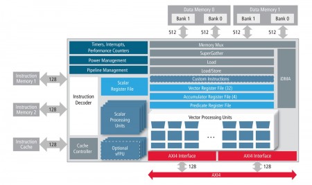
Image Architecture of the Tensilica Vision P5 core
“We have re-architected for five times less energy and reduced the number of cycles needed per pixel for low-level operations,” Crespo claimed. “Our memory interfaces are already pretty fast but we didn’t have the ability to do non-aligned accesses without using DSP instructions to realign them. The SuperGather engine in the P5 provides a massive increase in parallelism.
“SuperGather is very good for image de-warping and detection algorithms such as the Hough line transform.”
The SuperGather engine works by pulling data from a number of different, non-aligned memory locations in banks of local memory into a vector register so that one VLIW instruction can process the disparate data elements in one operation. The relatively small banks allow a number of locations to be indexed easily with one command. Typically, the algorithm will pull a window of interest from main memory and then use the SuperGather engine to manipulate data within the sub-bank.
“Of all the features in P5, this gives use the biggest bang for the buck,” Crespo said. “A lot of DSP instructions go away when you no longer have to realign data within the processor. You get rid of the need to do a lot of shift and select instructions, which reduces energy significantly.”
Floating-point addition
As well as adding the memory controllers, Tensilica provides the P5 with the option of a vector floating-point unit that supports the IEEE754 standard and will execute up to 16 instructions in parallel. “It bridges that gap between [desktop] GPUs and the processors generally used in embedded systems,” Crespo said.
The result for a full implementation of the P5 is a DSP that will perform 256 operations per cycle versus 96 for the previous generation, Crespo added. In a 16nm finFET process, the processor should hit 1.1GHz in terms of clock speed.
The SuperGather engine and floating-point support in combination with the ability to define custom instructions that the P5 continues to offer potentially opens up a market in scientific computing, Crespo claimed. By pulling data from multiple non-contiguous locations in one hit, the architecture is potentially much better at dealing with multi-dimensional, sparse matrices.
“Many of these applications were previously using GPUs. This architecture opens up a completely new market. We can offer one tera-operations per second in two square millimeters of silicon,” Crespo argued.
Support for floating-point operations would also provide an easier way to move neural-network code from a workstation to an embedded platform, he added.
