Ambipolar FETs are an each-way bet
We’re used to the idea of insulators, conductors and, vitally, semiconductors – materials whose electrical characteristics can be biased one way or another depending on the impurities with which they are doped – as the basic building blocks of devices such as FETs. Now it’s time to take another concept on board – the ambipolar device.
Scientists at the Swiss Federal Institute of Technology (EPFL) at Lausanne have demonstrated ambipolarity, the ability to switch between n-type and p-type conduction, in a nanoscale transistor made from silicon.
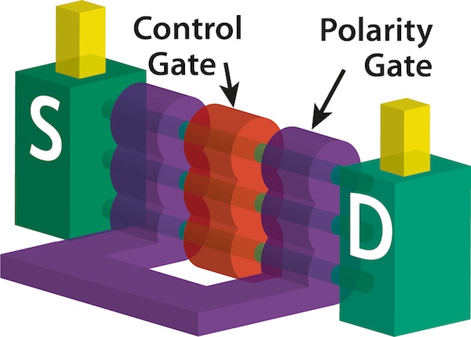
Here’s a schematic of the concept:
Although such an undecided material has traditionally been seen as a limitation for circuit design, the EPFL research team decided to try to turn the limitation into a virtue.
They built an ambipolar FET using a silicon nanowire on an SOI substrate, and surrounded it on all sides with a control gate. A pair of ‘polarity’ gates were used to surround either end of the silicon nanowire, and to switch it between n and p-type conduction.
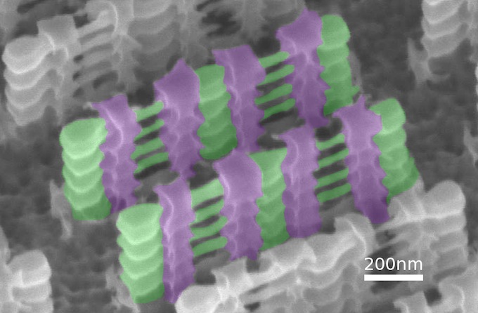
Here’s a tilted SEM of a multiwire device that has already had the polarity gates defined by deposition and etching:
The devices showed an on/off current ratio of 106 and a subthreshold slope of 70mV/dec. The researchers also used several of the devices to build an XOR gate.
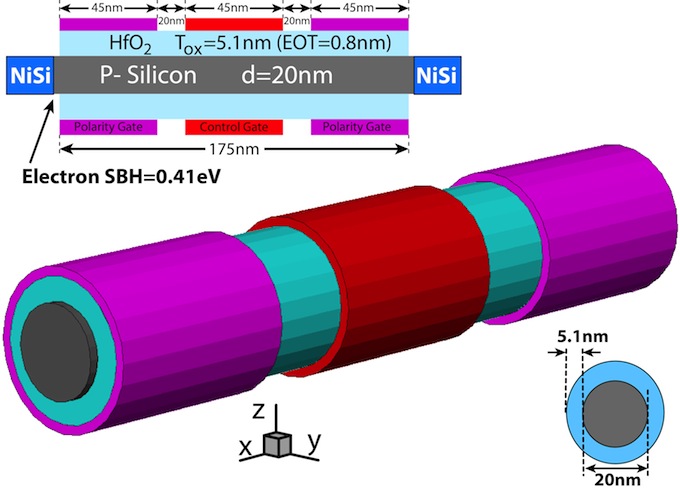
The EPFL team have also developed an idealised design for the ambipolar nanowire FET, shown here with three 45nm-long gate regions.
The ambipolar device is interesting, but does it matter? The history of semiconductor device development is littered with device structures that were interesting, but never quite made it to the mainstream, usually for practical reasons such as cost or complexity. What’s interesting about the emergence of this device now is that as we move beyond the 20nm process node the industry is beginning to have to think carefully about what it will do when it is no longer possible to control the flow of charge through a channel using a gate. At that point, all bets are off and the field for novel device architectures widens again.
There’ll be more on the ambipolar device in Paper #8.4, “Polarity Control in Double-Gate, Gate-All-Around Vertically Stacked Silicon Nanowire FETs,” M. De Marchi et al, EPFL, at the International Electron Devices Meeting in San Francisco this December.
Find out more about IEDM here.