20nm test demands new design-for-test and diagnostic strategies
20nm test needs new approaches to cope with short delay defects, new memory failure mechanisms and the consequences of test compression strategies
The introduction of 20nm manufacturing processes brings new yield challenges that influence design-for-test (DFT) strategies. At 20nm, defect densities higher, and there are significant on-chip process variations that affect transistor sizes, transistor threshold voltages, and wire resistances. These variations give rise to fault effects that are more difficult to model electrically but can no longer be ignored. To maintain the high quality of 20nm test and minimize the cost of test escapes, DFT techniques that target small delay defect (SDD) faults as well as a number of ‘new’ memory failure mechanisms are essential. In addition, to improve yield quickly, designers need to employ test structures in the scan compression logic to enhance their ability to test and diagnose these issues.
Let’s begin by looking at how slack-based at-speed testing is being used to efficiently target small delay defects.
Slack-based at-speed 20nm test
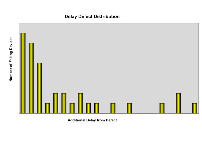
Delay defects add enough signal-propagation delay to produce an invalid response when a design is operating at its target frequency. Experimental data going back more than two decades [1, 2] have shown that most delay-defect failures are caused by SDDs, which affect only the smallest timing slacks in a design (Figure 1). On-chip process variations at 20nm adversely impact circuit timing in a higher percentage of devices, further skewing the delay-failure distribution toward smaller delays. Targeting these SDDs during manufacturing test will improve delay defect coverage and lower the test escape rate, as measured by defective parts per million (DPPM).
Figure 1
The distribution of defects in devices failing due to delay defects is skewed toward delays affecting the smallest timing slacks (Source: Synopsys – click image to enlarge)
The most predictable and pattern-efficient approach to SDD testing is to use SDD automatic test pattern generation (ATPG) algorithms to target SDDs, and standard transition delay (TD) ATPG algorithms to target longer-delay defects. In this combined approach, SDD ATPG only targets undetected delay faults along paths with timing slack below a certain threshold value, while standard TD ATPG targets any remaining undetected faults.
However, SDD ATPG needs highly accurate estimates of a design’s timing slacks. Requiring the ATPG tool to perform many thousands of timing calculations for each generated pattern would slow down ATPG run-time performance significantly and, more importantly, produce results that do not correlate with sign-off timing analysis.
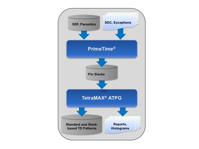
Synopsys’ slack-based at-speed testing solution (Figure 2) avoids these performance and accuracy issues. TetraMAX ATPG uses data generated by PrimeTime’s signoff timing analysis results to target SDDs with very high precision. Because PrimeTime models all the key process, physical, noise, and clock-network effects required for accurate timing analysis at 20nm, it is an essential part of the slack-based TD ATPG solution. The unified flow combining SDD ATPG and TD ATPG differs from the standard TD ATPG flow only in the requirement to import slack data from timing analysis to ATPG.
Figure 2
Synopsys’ slack-based at-speed test solution uses data generated by PrimeTime to target SDDs with very high precision (Source: Synopsys – click image to enlarge)
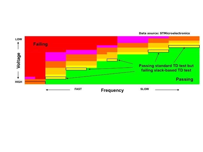
This approach to SDD testing has proven to be a highly effective and pattern-efficient means to achieve ultra-low DPPM levels on production designs. STMicroelectronics’ delay defect testing of hundreds of thousands of automotive ICs showed that 63% of parts failing due to delay defects were covered only by the SDD patterns [3]. The shmoo plot of voltage versus frequency is shown in Figure 3 for parts that passed the basic stuck-at tests.
Figure 3
Slack-based TD ATPG is more effective screening parts at various voltage-frequency corners than standard TD testing (Source: Synopsys – click image to enlarge)
The different colors represent the percentage of parts that passed both TD and SDD testing, with green designating 100% passing, red 0% passing, and the other colors intermediate percentages. The yellow regions with black boundaries signify voltage-frequency combinations where the parts passed the TD patterns but failed the SDD patterns.
After the evaluation, Synopsys’ slack-based at-speed testing solution was widely adopted across design groups at STMicroelectronics to improve the quality of production testing and lower the cost of test escapes.
Optimizations for embedded memory test and repair
Process variations at 20nm also lead to small delay defects in embedded memory sub-systems. SDDs in address decoders can activate or deactivate incorrect memory rows or columns. A dynamic memory fault can occur when there is enough difference in wire resistance between matched bit lines shared by a column of memory cells to cause a read failure. When there are process variations within a single memory cell – a scenario more likely to occur at 20nm – read, write, access, or hold failures can occur.
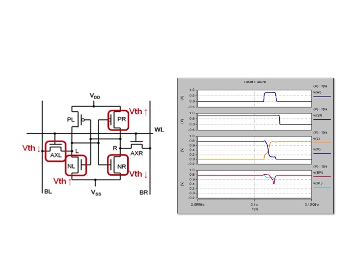
For example, in the 6-transistor SRAM cell shown in Figure 4, a read failure occurs when there is more than a 22% variation in threshold voltage across the devices.
Figure 4
To properly test for read failures due to process variation within a RAM instance, patterns need to be applied across multiple corners (Source: Synopsys – click image to enlarge)
Another fault effect that has emerged at 20nm stems from random telegraph noise (RTN). This effect is potentially more harmful at 20nm than at previous process nodes because there is a higher probability that RTN-induced failures will occur. Due to the random behavior of an RTN fault, multiple consecutive reads from each memory address must be performed to detect it.
The ability to automatically detect, locate, and repair these ‘new’ failure modes is critical for improving DPPM at 20nm. Synopsys’ DesignWare STAR Memory System has been re-architected with test and repair algorithms designed to provide fault coverage and repair capabilities for address decoder delay faults, dynamic faults, RTN-induced faults, and other types of memory failure modes stemming from process variations at 20nm and below.
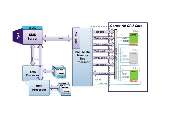
To maintain the performance advantages of the 20nm node, embedded memory test and repair solutions must interface with high-performance processor cores without compromising their speed. This means adding memory test and repair logic outside the cores while utilizing a processor’s existing shared bus interface and pipeline stages, adding additional pipeline stages as needed to meet a design’s at-speed testing requirements.
The new STAR Memory System architecture uses these techniques to enable at-speed test and repair of high-performance multi-core processors, eliminating the need for dedicated test wrappers (Figure 5). These and other optimizations reduce area of the memory test and repair subsystems by 30% compared with those implemented by the previous-generation architecture.
Figure X
Using the shared bus interface to the memories of an ARM Cortex-A9 processor core eliminates the need for dedicated test wrappers (Source: Synopsys – click image to enlarge)
Design for diagnostics
So far, we have focused on DFT methodologies and automation needed to achieve high defect coverage in the presence of new and unfamiliar failure mechanisms at 20nm. However, the fact that a design is testable does not ensure it is diagnosable. Design for diagnostics (DFD) strategies that make designs easier to diagnose are equally important at 20nm. This is because defect densities are higher at 20nm than at previous process nodes, making the ability to accurately identify defect locations and defect types in failing parts critical to quickly ramping up to high-yielding, profitable products.
To illustrate DFD, let’s examine how one technique improves the ability to diagnose failures in designs that utilize scan compression to reduce test costs.
Relatively higher defect density implies there is a higher probability that, during scan testing of a design, more than one scan chain will capture ‘faulty’ values – binary values different than what is expected if the chip were fully functional. (Implementing a large number of scan chains also increases the probability that multiple scan chains will contain faulty values.) With standard scan, the outputs of all the chains are directly observable and it is evident which chains have faulty values.
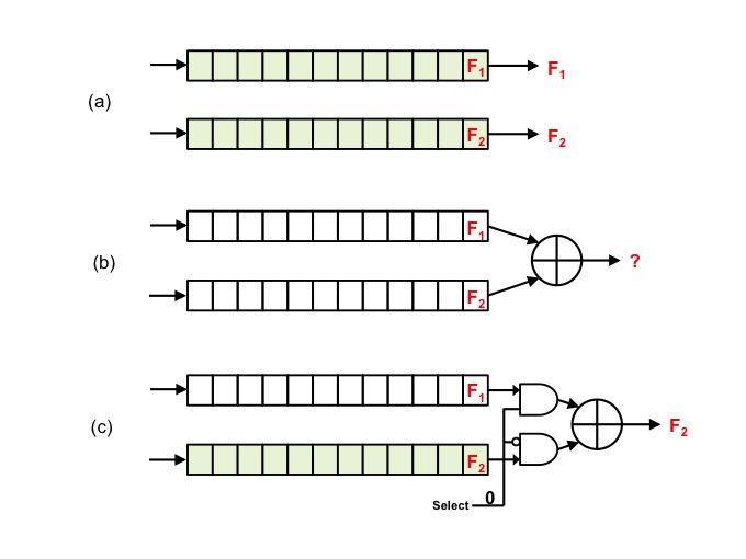
This scenario is shown in Figure 6a, where both faulty values F1 and F2 are directly observed at the scan chain outputs. Once the chains with the faulty values are identified, the diagnostics tool can trace backward through the logic cones to determine the source of the faulty behavior.
In contrast, scan compression uses XOR gates to compress the chain data instead of directly observing it. But relatively few observation points makes it more difficult to determine with certainty which chains have faulty values due to the aliasing effect shown in Figure 6b.
The DFD logic shown in Figure 6c, inserted by Synopsys’ DFTMAX compression, isolates the defective scan chains by observing only one of the faulty values (F2) through the observation point shown. If there is another available observation point (not shown), the other faulty value (F1) can be propagated to it in the same shift cycle. An addition benefit of isolating scan chains in this manner is that it provides TetraMAX ATPG the ability to manage unknown values (X’s) captured across multiple scan chains, thereby improving test coverage without significant pattern inflation in the presence of X’s.
Figure 6
You can diagnose both faults when the scan-chain outputs are directly observable (a), but can’t when they are scanned into the same XOR gate at once (b). The configuration in (c) makes it possible to determine which faulty value belongs to which scan chain (Source: Synopsys – click image to enlarge)
It is also beneficial to use the above DFD method for chain diagnostics designed to isolate ‘chain defects’ that affect scan chain shifting. Because scan chain shifting requires a significant portion of the chip to be fully functional – sequential elements, clock tree and power networks, scan inputs and outputs, synchronous set/reset logic, test control logic, and scan chain logic – chain diagnostics are an effective way to speed yield ramp and debug failing parts at 20nm where defect densities are relatively high. TetraMAX ATPG generates specific chain test patterns to enable more accurate diagnostics, identifying both the failing logic and the defect type when multiple scan chains are defective.
Conclusion
Although the shift to 20nm processes provides designers the opportunity to pack more than 20 billion transistors onto a chip, it also introduces new yield challenges that will require innovative DFT and DFD strategies to maintain low DPPM and facilitate accurate diagnostics. Synopsys’ slack-based at-speed testing has been proven to be more effective at targeting SDDs than standard transition delay ATPG. For test and repair of embedded memory sub-systems, the STAR Memory System provides a new optimized architecture that interfaces seamlessly with high-performance processors and targets not only static and dynamic faults, but also process variation and RTN-induced failures. Finally, DFTMAX compression and TetraMAX ATPG work in tandem to enable accurate chain diagnostics for accelerating yield ramp at 20nm.
References
- Nigh, P., and A. Gattiker, “Test Method Evaluation Experiments & Data,” Proceedings of the International Test Conference, 2000, www.ieee.org. pp. 454–463.
- Park, E.S., M.R. Mercer, and T.W. Williams, “Statistical Delay Fault Coverage and Defect Level for Delay Faults,” Proceedings of the International Test Conference, 1988, www.ieee.org. pp. 492–499.
- Mattiuzzo, R., Graniello, S., Talluto, S., Conte, A., Cron, A., “Small Delay Defect Testing,” SNUG Europe Proceedings, 2007, http://www.synopsys.com/Community/SNUG/Pages.
Author
Chris Allsup is marketing manager in Synopsys’ synthesis and test group. He has more than 20 years of combined experience in IC design, field applications, sales, and marketing, and has authored numerous articles and papers on design and test.
Company
Synopsys700 East Middlefield Road
Mountain View, CA 94043
Phone: (650) 584-5000 or
(800) 541-7737


Chris, in my experience diagnosing defects, a big problem was that, especially early on, we would see a whole lot of failures and it was very time consuming pinpointing the defect. How have your tools solved this problem?
Abraham – I work with Chris on the test tools at Synopsys. The general answer to your question is “yes”. For scan-based designs, our tools provide diagnostics of the tester generated failure data, as well as yield analysis across mulitple die. Our field teams can provide more info if desired.