Design for test: a chip-level problem
The inherent complexity of today’s system-on-chips, with their multiple clock and voltage domains, requires test considerations to be moved further up design flows. The article describes strategies for and benefits from apply test before RTL goes through synthesis, augmenting what is already achieved through memory built-in self test and automatic test pattern generation.
Mark Twain said, “Everyone talks about the weather but nobody does anything about it.” Design for test (DFT) is a bit like that.
We pay lip service to the fact that every chip needs to be tested as well as manufactured, but somehow all the glamour goes into simulation, synthesis, place and route, and other aspects of design creation. But ignoring a problem does not make it go away. It really is true that every chip needs to be tested. With testers getting more and more expensive, and test times increasing as chips get larger, the cost of test is not a negligible component of the overall production cost.
Historically, the way designers have handled test has been largely to ignore it. It was assumed that test was a process that could be grafted on after the design was complete. The increasing prevalence of memory built-in self test (BIST) and scan chains with automatic test-pattern generation (ATPG) for logic has meant that most aspects of test would be left to a specialist test expert when the design was largely complete.
That approach worked well enough in the world of smaller chips with single clock domains, single voltage domains, low clocks speeds, relatively generous power budgets, and not too many worries about congestion or signal integrity. SoCs today are not like that. Yes, it is true even today that not every project has to deal with all of these complications. But most system-on-chips (SoCs) are large, have large numbers of clocks, multiple voltage domains and so on. In our world, leaving test until the end is a recipe for surprise schedule slips just before tapeout.
It is also important to note that it is a chip that gets tested. We can use various techniques to get vectors to blocks, but ultimately it is a chip that sits on the tester and not a block, and so test is a chip-level problem. And, not surprisingly, chip-level problems are best handled at the chip level.
The solution to these conundrums is to handle synthesis at the chip level and make your DFT strategy an integral part of that. It means that we address the problem earlier in the design cycle and at a higher level.
Moving test up the flow
The first part of handling DFT in this way is to check the RTL before synthesis.
There are some RTL constructs that lead to gate-level structures that are inherently untestable with a standard DFT methodology. One good example is asynchronous set/reset or clocks that lack controllability. In addition, the commonly used power reduction technique of clock gating changes a DFT-friendly structure into a problem that needs to be solved by using clock-gating cells with an additional test pin.
When it comes to actually linking up the scan chains, there are a number of complications that need to be addressed or optimized since different flops may have different power supplies or clocks and so cannot just be naïvely hooked together.
Scan chains can cross power domains, such as areas of the chip with different power supply voltages or areas that can be powered down. For such domains, level-shifters and isolation cells need to be inserted automatically at the boundaries. This is driven of course by the file that specifies the power policy and defines the separate power domains, be it expressed in the CPF or the UPF standard.
Clock domains also need to be taken into account: that is, the areas are controlled by different clocks during normal (i.e., “non-test”) operation of the chip. Sometimes, one solution is simply to restrict scan chains to individual clock domains. But that is not always desirable. Specifically, there are two cases to consider.
If the two clock domains do not interact during normal operation of the chip, then different clock trees may end up with different timing, creating hold violations. To avoid these violations, lockup latches need to be inserted. These latches hold the value on the inverted value of the clock and so ensure that the value is available downstream without any race condition.
The second case is when clock domains do interact during normal operation. In this case, they should already be synchronized correctly and then can be treated as identical during scan chain generation without causing any problems.
To make better use of tester resources, scan test programs are almost always compressed. This requires placing a test compression block on the chip. These designs are proprietary to each ATPG vendor such as Mentor Graphics with its Tessent TestKompress tool suite.
Test compression blocks allow a comparatively small number of test pins coming onto the chip to be used to generate perhaps hundreds of times more scan chains, shortening test times as well as minimizing test pin overhead. In practice, the test compression structure is a block of RTL created by the test compression software that is then added to the RTL for the whole chip and hooked up to the chains.
The flop factor
But the biggest challenge that needs to be taken into account when creating scan chains is the physical location of the flops. It is here that working at the chip level really offers a big advantage over working at the block level and then manually hooking up the sub-chains. The scan chains are not limited by the logical hierarchy of the design. During physical design a particular logical block may end up being placed in a compact region that is good for scan insertion, but when it is not, it may end up spread out across the whole chip with the scan chain stretched out everywhere.
Another advantage of doing scan insertion during synthesis is that potential test problems can be debugged early in the design cycle. Since test, and especially scan chain reordering using block-based methodologies, occurs late in the design cycle, unexpected problems almost always have an impact on the final tapeout schedule.
Figure 1 shows a design where the scan chains have not been ordered in a way that takes into account their physical placement after synthesis.
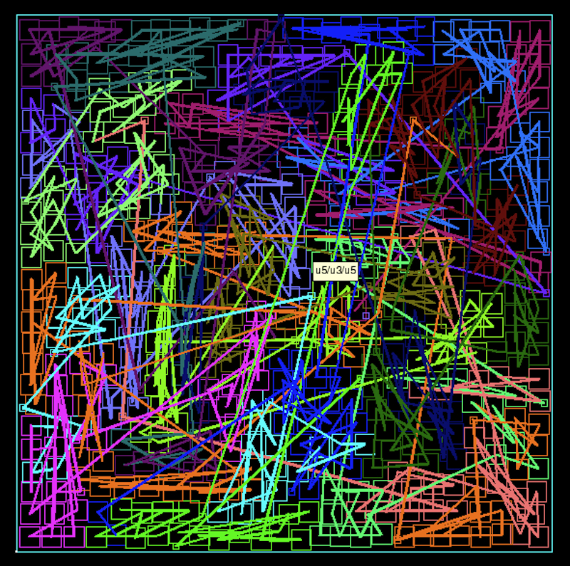
Figure 1
Small design with scan chains that do not account for physical placement
Source: Oasys Design Systems
Figure 2 is the same design re-implemented making use of the physical placement information. Each scan chain is a different color so the advantage in terms of routing is clear.
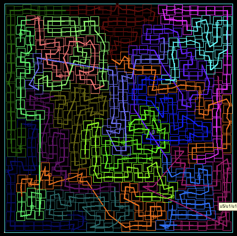
Figure 2
Design from Figure 1 taking advantage of placement information during synthesis
Source: Oasys Design Systems
Figure 3 is not a piece of abstract art but is a much larger design where the scan chains were hooked up using only logical information.
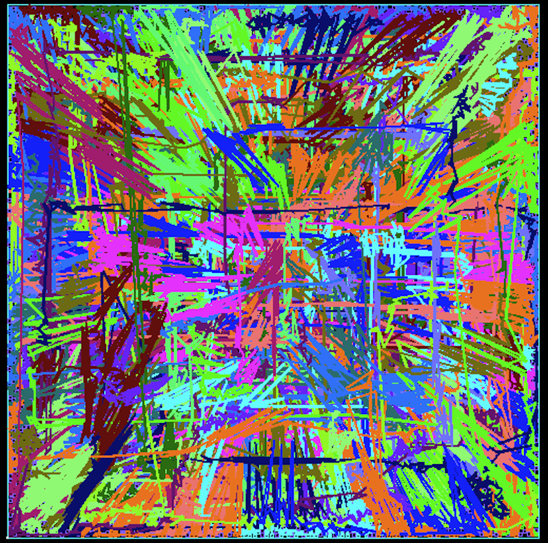
Figure 3
Large design that does not use placement information during scan insertion
Source: Oasys Design Systems
Figure 4 is the same design using physical placement information during synthesis. Most chains are compact enough that they look like separate areas on the die.
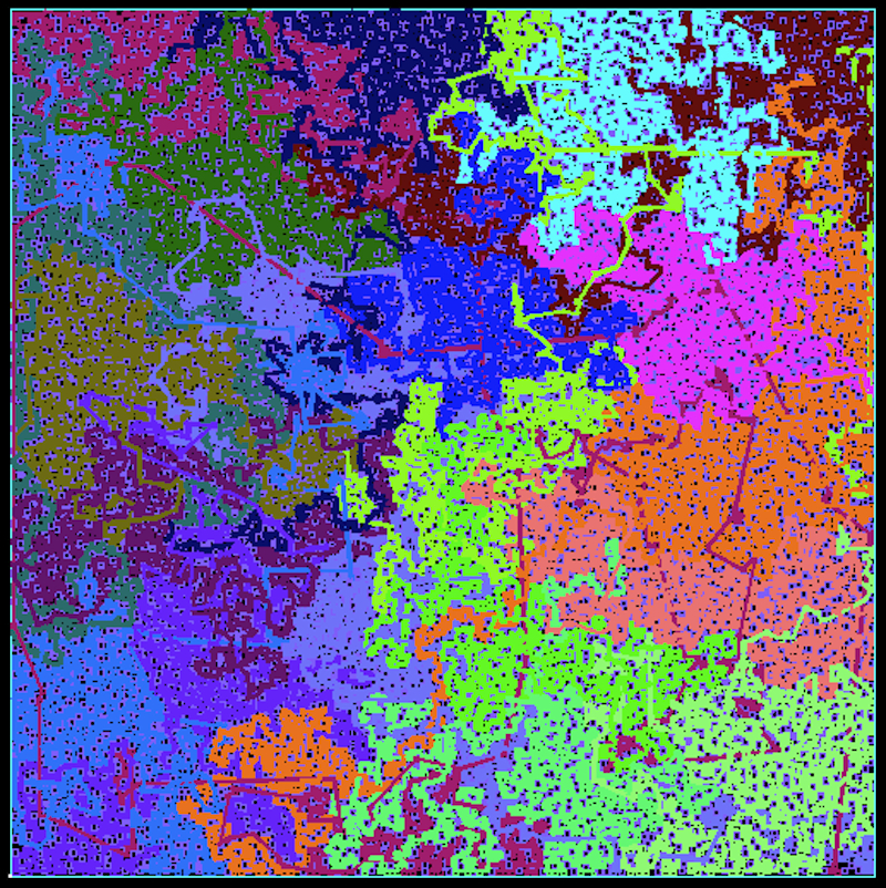
Figure 4
Design from Figure 3 taking placement information into account during synthesis
Source: Oasys Design Systems
The output of generating the scan chains is a standard ‘scandef’ file that can be used by both downstream physical design tools and ATPG tools. The user may choose to do another round of scan-chain ordering after physical placement.
Increasingly, large parts of chips are not synthesized directly but are blocks of IP from third-party suppliers. The standard way to handle test for such blocks is to provide test information using the Core Test Language (CTL) IEEE1450.6 standard. It communicates the existing scan chains and how they are hooked up, and then allows for them to be merged into the top level scan chains.
RealTime Designer
Chip synthesis needs to be a high-capacity and very fast turnaround process. Oasys RealTime Designer can handle 100,000 flops per minute for analysis and runs at about half that rate for insertion. So, a 10 million-instance design that might contain one million flops can be processed for scan insertion in around 10 minutes for analysis and 20 minutes for scan insertion.
Figure 5 shows the DFT flow and the various files that are used to create the final DFT placed netlist and test program.
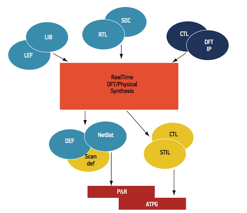
Figure 5
DFT flow and files
Source: Oasys Design Systems
By operating at a high level, test insertion can be treated as a global problem and a more suitable DFT architecture can be chosen. Performing scan insertion during synthesis means that it is not necessary to leave the tool, and the full-chip view makes it easy to do full-chip analysis and optimize the overall architecture. This in turn leads to shorter test times, smaller die, and fewer secondary problems.
The apt comparison here is with the traditional approach of carrying out test at the block level where decisions need to be locked down early on as to how many scan chains are in each block; with the full-chip view, this is completely automated.
Oasys Design Systems 3250 Olcott Street Suite 120 Santa Clara CA 95054 USA T: 408-855-8531 W: www.oasys-ds.com