Streamlining analog fault simulation
There has been automated fault coverage for digital circuits for some time now, but progress on the equivalent for analog circuits has been painfully slow. Test time per analog transistor has barely fallen in the last 20 years.
The reasons for this slow progress are well known. As test times for digital circuitry have progressively shortened, they have arguably provided a sufficient productivity boost even as simulating all the possible faults in analog circuity has continued to take an uneconomically long time. Meanwhile, there has also been no industry-accepted analog fault model around which innovation could coalesce.
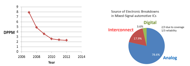
As Figure 1 shows, the industry has now reached a crunch point. From 2010 onwards, work toward reducing test escapes (defective parts per million – DPPM) has become stranded on a plateau. At the same time, analog has grown to reach almost 80% as a source of electronic breakdowns in mixed-signal automotive ICs – a segment broadly representative of the overall challenge.

Figure 1. Test escapes (DPPM) and breakdown sources for a mixed-signal automotive IC (Gielen et al, ITC 2014)
Academia and industry have been responding to the two challenges and more coherent progress is now being made.
A common fault model
A group of about a dozen companies began work on agreeing an industry-standard fault model in 2014 and hopes to deliver the components for an IEEE standard by 2018. But it has proved a challenging task delivering something as straightforward as the stuck-at model that has proved so adaptable for digital circuitry.
In a Mentor Graphics White Paper, Stephen Sunter, the company’s engineering director for mixed-signal DFT, has reviewed some of the issues that arise:
Simulating only short and open defects has not been accepted because analog design is inherently about tolerating variations and because manufacturing experience has shown that some ICs are defective because of parametric defects. A test that detects all opens and shorts might miss some defective variations.
Simulating defective variations in circuit elements has not been accepted because to achieve acceptable yield, designers already use Monte Carlo simulations to ensure a design can meet all specifications in the presence of all expected variations in process, voltage, and temperature (PVT). Semiconductor wafers contain process control monitors (PCMs), which are small standard circuits on the wafer for measuring to ensure process parameters across the wafer are within specification. As a result, most defects seen in manufactured ICs are shorts and opens (except in the most advanced process nodes).
Simulating defective variations in high-level models of basic analog functions (such as op-amps, filters, and ADCs) has not been accepted because there is no way to delineate a sufficient set of defects, the defects do not correlate to silicon defects, and creating these models and defective variations is a difficult and non-automated task.”
Sunter notes that there is then a further debate over preferences for company-specific design-for-test strategies versus other users who simply want to apply a generic best-in-class approach.
The work, as they say, continues.
Reducing analog simulation time
Academic and industrial research aimed at reducing unwieldy analog simulation time has highlighted a number of techniques that could each help somewhat, as well as proposals for reducing the number of defects that need to be simulated. As identified by Sunter, these are:
Six simulation strategies
- Simulate only sorts and opens in the schematic netlist, without variations.
- Analyze a circuit’s layout to find the shorts and opens that can actually occur (and the likelihood of those defects occurring).
- Simulate only in the AC or DC domain.
- Simulate the sensitivities of each tested performance to variations in each circuit element.
- Use a simplified, time domain simulation, such as fault sensitivity analysis (FSA), to measure the impact of injected shorts and opens on output signals only within the same clock cycle.
- Measure the current interrupted by each injected open or flowing though each injected short, or measure toggle coverage.
All these strategies have strengths but also significant weaknesses. There is no magic bullet.
For example, simulating only in AC or DC is very efficient where you are simulating open, short and variation defects but the technique does not work for mixed-signal circuits such as PLLs. Similarly, using FSA can reduce simulation times by 100X but, because of its restriction to a single clock cycle, miss those defects that affect outputs in subsequent cycles.
Such shortcomings can mean that there are still a great many issues and faults that may require further and time-eating manual defect analysis after the simulation run, certainly when these techniques are used in isolation.
Four ways to reduce simulated defects
- Randomly select defects from a list of all potential defects.
- Randomly select defects after grouping them according to defect likelihoods, also known as stratified random sampling.
- Select only the principal parameters of the circuit elements.
- Select representative defects based on circuit analysis.
As before, each of these tools can help to control the defect simulation count but can involve trade-offs in terms of accuracy or the volume of defects reported.
The state of the art with Tessent DefectSim
As the plethora of options above suggests, along with the current lack of a standard analog fault model, the best solution lies both in mixing and matching the proposed techniques and refining or building upon them. It also requires a platform that the user can tailor to his or her particular requirements and flow, where necessary.
This is the approach Mentor Graphics has taken in developing Tessent DefectSim. As Sunter explains, “Simulation time is reduced using a variety of techniques that combine to reduce total simulation time by many orders of magnitude compared to some of the previous approaches, without introducing a new simulator or reducing existing simulator accuracy.”
Similarly, when it comes to the analog fault model, “[It] can be shorts and opens, just variations, or both. Or designers can substitute their own proprietary fault models.”
And as for targets, “The defects can be injected at the schematic level, at the layout level, or a combination of both.”
Tessent DefectSim’s use of a technique called likelihood-weighted random sampling (LWRS) illustrates how Mentor has built upon existing proposals, here with a new statistical technique that is equivalent to stratified random sampling (#2 on the list of defect reduction options). Sunter describes how it works:
Each stratum contains only one sample (defect). The likelihood of randomly selecting any given defect is proportional to the likelihood of the defect occurring. Each likelihood of occurrence is computed based on designer-provided global parameters, and parameters of each circuit element. For example, shorts are “the most dominant”. In state-of-the-art production processes, shorts are 3~10X more likely than opens.
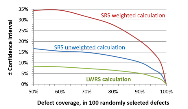
When the range of defect likelihoods is large, as it is for mixed- signal circuits, LWRS requires up to 75% fewer samples than SRS for a given confidence interval, as Figure 2 shows. In practice, when coverage is 90% or higher, this means that it is usually sufficient to simulate a maximum 250 defects, regardless of the circuit size or the number of potential defects, to estimate coverage within 2.5%, for a 99% confidence level. Simulating as few as one hundred defects is sufficient to get ±4% estimate precision. For small circuits, or when time permits, all defects can be simulated.
Tessent DefectSim is highly flexible. A user working on a linear circuit can opt for the more efficient AC and/or DC mode simulation (#3 on the list of simulation strategies). However, for those designs like PLLs, there is the option of simulating in a time domain (transient) mode. Then, for the fault model, the user can opt for shorts and opens, just variations, or both – or indeed substitute a proprietary model.
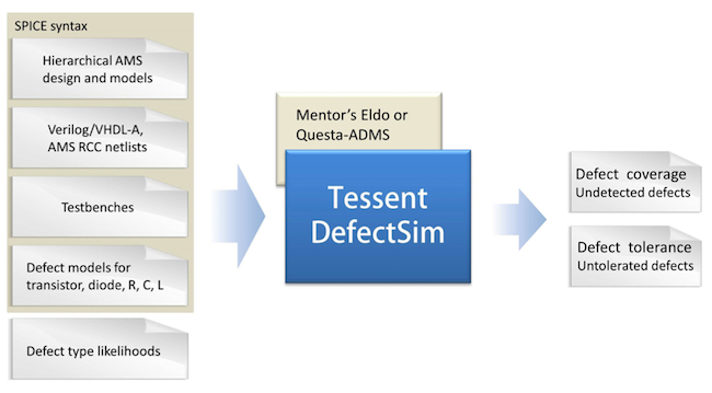
You take everything that might help and use it as appropriate, but Tessent DefectSim also does this within the context of familiar tools and technologies, specifically the existing Eldo and Questa-ADMS simulators. An overview of the flow is shown in Figure 3.
The strategy behind Tessent DefectSim is already achieving wide recognition: the tool recently collected the ‘Product of the Year’ award from Electronic Products magazine. If you want to know more about the technologies at its foundation and how the Mentor team has sought to optimize them, Stephen Sunter has embarked on a three-part White Paper series, the first part of which is extensively quoted here.


