Directed self assembly may offer similar benefits to EUV, process modeling study says
Directed self assembly (DSA) techniques may offer similar advantages in terms of process variation control as EUV lithography, according to a study carried out using 3D behavioral process modeling techniques.
This could reduce fab cycle times, ease process integration and save costs in advanced semiconductor processes, especially for DRAMs, whose regular structures are well-suited to the use of DSA.
Speaking during this week’s SPIE Advanced Lithography conference, David Fried, CTO – semiconductor, at 3D process simulation company Coventor, said: “What we’re seeing, without [the availability of] EUV, is that every critical patterning layer is being done with multiple lithography passes, using either self-aligned quad patterning (SAQP) or multiple litho-etch (i.e., LE2 or LE4) passes.
“All of those passes on the lithography equipment are expensive. But, if you look one step deeper [than just the litho steps], there are many additional deposition and etch processes in these multi-patterning schemes – so there is more of everything.”
One of the major issues with SAQP and LE4 approaches to patterning, apart from cost, is their complexity, which tends to lead to the complex interaction of many small process variations turning into larger issues. According to Fried, patterning a critical layer with SAQP could take 30 to 50 individual process steps – depending on the approach to deposition, etch and cleaning – up to ten times more steps than using DSA or EUV.
“The biggest bang for the buck in using EUV and DSA is control of variation,” he said. “DSA has the potential to offer some of the same variation improvements that EUV does, because of the reduction of integration steps necessary, if it can deliver at the unit process level.”
Fried said that one of the key things he would be looking at during SPIE is the progress on improving the variability control of EUV and DSA unit processes.
“EUV seems to be getting there from a process control point of view. DSA, from a unit process control standpoint on issues such as line edge roughness (LER) and critical dimension (CD) control, seems to still be well behind EUV.”
In a paper to be presented at SPIE, Dr Mattan Kamon of Coventor will present new work on exploring the use of DSA techniques in a possible future DRAM process.
“In this work, we have taken apart an advanced DRAM flow to say ‘Where would we put DSA?’,” said Fried. “We’ve chosen two critical patterning layers: in the active area patterning, which might otherwise be done with SAQP, and in the capacitor patterning, which might otherwise be done using LE4.”
Using some assumptions about eventual DSA process control, the Coventor team applies process-predictive behavioral models of each step in the process (rather than using full physical models that would take too long to run), and has undertaken multiple simulations of the resultant process including various sources of process variation. The new DSA behavioral models have been previously demonstrated in a logic technology flow, but this is the first demonstration in a DRAM process. Automated virtual metrology and structural checking is implemented to gauge success or failure of the integrated DRAM. The contact area between source/drain and the charge-storage capacitor is used as a metric for the impact of those process variations on the fully-integrated DRAM structure.
“This contact-area variation is a measure of unit-process success in a truly integrated context,” said Fried.
The work compared two DRAM flows – one using SAQP and the other using DSA on the active area patterning, as shown here:
Figure 1 An SAQP based DRAM flow - click to animate (Source: Coventor)
Figure 2 A DSA based DRAM flow - click to animate (Source: Coventor)
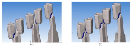
The critical contact area used as a proxy for variability control is shown in blue in Figure 3:
Figure 3 Points of contact between source/drain and capacitor in SAQP (a) and DSA (b) processes (Source: Coventor)
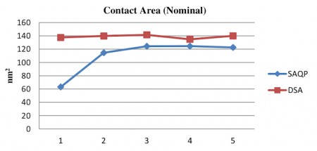
Variation in these contact areas is shown in Figure 4, in which the first contact (1) made with an SAQP approach has less than half the area of the same contact made using DSA. Overall variation in the DSA process, compared with the nominal result, is less than 5%.
Figure 4 A DSA-based approach kept contact area closer to the nominal values than SAQP (Source: Coventor)
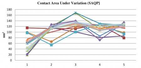
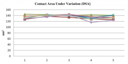
Coventor also simulated the impact of various forms of process variation on this critical contact area, for the two different approaches:
Figure 5 Contact area variation in an SAQP based process under various process variations (Source: Coventor)
Figure 6 Contact area variation in a DSA based process under various process variations (Source: Coventor)
Fried commented: “DRAM process margins are razor thin. If you’re in a process margin constrained environment, this study shows that DSA may offer integrated advantages.”
This work also demonstrates the implementation of a DSA process to pattern the hexagonally close-packed capacitor array, which would otherwise demand multiple lithography-etch cycles. This is the first demonstration of the use of Coventor’s DSA models for this type of pattern.
“The higher-level message is that patterning is the entire battleground now, where yield is being gained or lost, and the ability to model these variation issues on patterning schemes and full process integration is essential.”
