Synopsys puts physical IP prototypes into developers’ hands
Synopsys is launching FPGA-based IP prototyping boards to join its existing HAPS family of system prototyping solutions. The idea is to make it easier both to share physical prototypes of IP blocks and subsystems with developers who need to work with real hardware, and to make it easier to integrate those blocks into a system-level prototype.
According to Mick Posner, director of product marketing, FPGA-based prototyping solutions at Synopsys, the company has made 500 of its HAPS-70 system-prototyping solutions since the product’s launch in October 2012, and sold more than 450 of them. It has also found that leading customers have quickly taken up its largest capacity, 144M ASIC gate, variants within three months of launch.
But with the increasing use of IP and the growing importance of proving that IP using real-time data, Synopsys has also seen a growing need for prototyping much smaller blocks than would fit sensibly into its lowest-capacity HAPS-70 12 offering.
“What we found was that there was a step before HAPS-70 12, where smaller blocks were being validated,” said Posner.
The launch of HAPS-DX, for Developer eXpress, serves this need, providing capacity for IP prototypes of up to 4M ASIC gates – enough, Posner argues, to accommodate 80% of today’s complex IP blocks.
“These systems enable early software development and early hardware/software validation,” said Posner, especially in situations where IP and SoC development are separate so that there is a strong need to validate an IP block, its interfaces and software interoperability before handing it off for SoC integration.
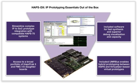
The common heritage of HAPS-DX and the HAPS-70 system eases the physical integration of proven IP blocks into a system FPGA prototype, simply by plugging the –DX board carrying the IP into the larger -70 system. Synopsys is also including a tool suite with the HAPS-DX, including optimized software for FPGA synthesis, debug and clock optimization.
This last is one area where using FPGAs to prototype IP that is ultimately targeted for an SoC can go wrong.
“Ninety per cent of the failures [of FPGA prototyping efforts] that we see are because of a lack of understanding of how to move from ASIC code to FPGA code,” said Posner.
For example, the gated clocks and clock trees that an IP designer might use to control power in an ASIC target don’t map directly into an FPGA. Similarly, power intent as expressed in a UPF file may need to be interpreted differently for an ASIC and an FPGA. The toolchain also supports the SDC format for timing intent.
Figure 1 Synopsys HAPS-DX for physical IP prototyping
The HAPS-DX tool suite also includes the HAPS Deep Trace Debug facility, which can store seconds of signal trace data thanks to memory on the HAPS-DX board (rather than having to use the FPGA’s memory), and Synopsys Verdi for debug visualization.
Because HAPS-DX builds on the HAPS-70 infrastructure, users will be able to access a wide range of HAPS daughter boards, as well as FPGA Mezzanine Cards, as well as prevalidated IP from the Synopsys DesignWare offering.
The inclusion of Synopsys’ Universal Multi-Resource Bus (UMRBus) will also enable hybrid prototyping, by providing a connection between HAPS and Synopsys Virtualizer-based virtual prototypes for pre-RTL software development.
There are also optional transactors for ARM’s AMBA interconnect to directly interconnect a HAPS-DX system and Virtualizer Development Kits generated using Synopsys’ Virtualizer toolset.
In a statement, John Koeter, vice president of marketing for IP and systems at Synopsys, said: “With HAPS-DX, we are helping prototypers increase productivity by providing reuse of the implementation design flow, pre-validated DesignWare IP, and synthesis and debug software, which are all plug-and-play compatible with HAPS-70 systems.”
Further info
Related Expert Insight
