May 1, 2009
The earlier in a design cycle a decision can be made, the shorter the development time and the lower the development cost. This is probably the most important product development principle, and is especially true when interconnects are not transparent and signal or power integrity could be holding back performance. You must find, fix and […]
March 1, 2009
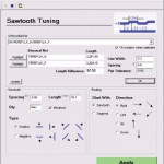
Length matching within a differential pair can be one of the more tedious tasks facing a PCB designer. This article describes how a team at communications and consumer electronics semiconductor company Broadcom overcame this by using the automation options available within their design tools. While the article describes automation tailored to a specific task, the […]
November 1, 2008
New tools and standards encourage communication between the electrical and mechanical domains, says Pawel Chadzynski. Most major electronics companies have separate electrical (ECAD) and mechanical (MCAD) design organizations. Efficient collaboration between these teams throughout the PCB design process can significantly reduce cycle times, lower the risk of re-spins, and improve quality. The first challenge to […]
November 1, 2008
This special edition of EDA Tech Forum Journal concentrates on PCB design. It’s an exciting area technologically right now, and we hope that the editorial content reflects that. One theme that kept emerging was that many of the contributors believe their discipline is at some sort of tipping point. And these changes don’t just come […]
Article | Tags:
November 1, 2008
Emerging technologies and markets could spur PCB tool growth despite economic concerns, says Mary Ann Olsson The worldwide PCB EDA software market maintained fairly stable 3.4% growth in 2007. Sales reached $532.5M, from $514.7M in 2006. The projected growth rate for PCB software in 2008 is 2.3%, bringing sales to $544.7M (Figure 1). One key […]
November 1, 2008
Floorplanning informed by thermal analysis can significantly improve PCB layouts, writes Robin Bornoff The number of PCB design constraints seems ever increasing. The risk that a design will fail either functional performance or reliability goals grows for each generation. One increasingly popular trade-off addresses a balance between thermal compliance and signal integrity. Components with high […]
November 1, 2008
The contributor supplies high-end military communications systems to both the US and Canadian Navies and here describes the development of a new methodology and also a new backplane for a system that is now being retrofitted onto all ships in Canada’s fleet. The project represented a tipping point. In specific terms, the changes were undertaken […]
November 1, 2008
New PCB tools have the intelligence to cut time and cost, explains Mark Forbes As far back as Marconi himself, RF design has been seen as having a touch of magic associated with it. Designs that looked just fine on paper would often require empirical tweaks to make them work properly. Until recently, even circuits […]
November 1, 2008
OSMOSIS is a super-fast optical switch developed through the Advanced Simulation and Computing program. The article describes the strategies adopted by the IBM team charged with designing the Central Scheduler board for the project. The design was of a far greater complexity than the team had previously encountered, and as a result, developed new pre-preparation […]
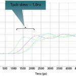
November 1, 2008
This paper builds on “Timing Numbers In ICX – What do we do with them?” [1]—a paper presented at the 2006 Mentor Graphics User2User conference (and now available for download at the journal’s Web site, www.edatechforum.com). The original paper focused on the need for timing analysis and the theory behind it; this paper takes a […]