Defying the downturn
 Emerging technologies and markets could spur PCB tool growth despite economic concerns, says Mary Ann Olsson
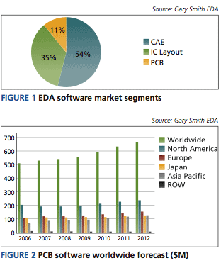
The worldwide PCB EDA software market maintained fairly stable 3.4% growth in 2007. Sales reached $532.5M, from $514.7M in 2006. The projected growth rate for PCB software in 2008 is 2.3%, bringing sales to $544.7M (Figure 1).
One key contributor to performance last year was the 24% growth in PCB software sales in Asia Pacific. This was bolstered by 10% worldwide growth in semiconductor revenue, and 5% growth in worldwide electronic equipment revenue.
Since the first quarter of 2008, US economic news and data have followed a steadily downward trend at an unsettling pace and EDA faces the knock-on effect.
This trend could seriously impact electronics industry growth, slow demand for PCB software tools, and lead to declining revenue growth during the forecast period. However, the broader electronics industry numbers are encouraging.
Worldwide PCB shipments remained fairly strong, with growth in the 4% range and capacity utilization ranging from 85 to 95% by June 2008. The growth rate in semiconductor shipments was up from 9 to 12% driven by wireless communications and computing, as well as the industrial (medical) segment and military applications.
The year-end forecast from WSTS is for 4% growth in worldwide chip revenues. While the US market is expected to remain volatile year and may have a influence on other regional economies through the first half of 2009, we believe there are abundant opportunities for investment in PCB software tools for emerging regions and technologies.
Forecast
The digital world has piled more and more complexity on the shoulders of device and package engineers.
Since the PCB software tool industry only recently started to migrate to enhanced suites for advanced high density interconnect (HDI) modules, complex SoC and embedded designs, our growth expectations for 2008 and 2009 remain cautious. PCB software revenue will increase slightly by 2.3% in 2008 to $544.7M based on stable market growth in Asia Pacific, China and India. More sustained growth is expected to drive overall PCB software revenue to $560.5M in 2009.
As more designs target nodes below 65 and 45nm, increased clock speed and faster switching speeds, lower power needs, over-design costs, chip-to-package delays, and complex PCB constraints will become market obstacles and breaking points for traditional board tools. But they will also drive innovative co-design solutions.
Today’s complex designs create a need for consistency along the entire design channel. Co-design solutions have become critical tools for engineers creating 65nm chip designs in emerging system-in-package (SiP) formats on multilayer boards. The new buildup technologies for using stacked, SiP, CSP, flip-chip and wafer level packages are expected to lift the US PCB software growth rate above 6% in 2010 and worldwide revenue to $593.6M million.
The emerging 3D and thru silicon via (TSV) package designs coming to the wider market in the 2011-12 timeframe will drive next-generation PCB design tool solutions and worldwide PCB software vendor revenue to over $668M (Figure 2).
Mary Ann Olsson is a chief analyst for Gary Smith EDA. More details about the company’s services to the semiconductor industry can be found online at www.garysmitheda.com.