More efficient board design for RF, analog and digital
 New PCB tools have the intelligence to cut time and cost, explains Mark Forbes
As far back as Marconi himself, RF design has been seen as having a touch of magic associated with it. Designs that looked just fine on paper would often require empirical tweaks to make them work properly. Until recently, even circuits that had been simulated virtually would always seem to need more than one pass during PCB design before they would function as expected.
One major obstacle to the transfer of RF circuits to PCBs has been the need to preserve not just impedance and ground-plane requirements, but also printed passive components. PCB design software was completely ignorant of the RF requirements until just a few months ago. That this knowledge has now been inserted into tools is good news for both RF engineers and PCB designers. Virtually every application space—consumer, telecommunications, military and aerospace, automotive, PC—has a growing RF content, with multiple standards (e.g., Wi-Fi, WIMAX, Bluetooth, GSM, 3G, GPS, etc.) needing to be accommodated on even the most standard mixed-signal boards.
The magic of RF
One of the most significant problems with moving simulated RF circuitry to a PCB at RF frequencies (especially microwave frequencies) is that printed metal shapes actually function as passive circuit elements. When PCB design software did not account for this, and layouts were then moved or scaled, the resulting shape was not at all what the RF circuit needed. The result was equivalent in an analog circuit to a 100? resistor suddenly becoming a 33k? resistor on being moved to the other side of the PCB—not a good thing.
PCB design software primarily understands metal on the substrate as a connectivity medium. There are cases, such as impedance matching, where the software comprehends that the metal serves more than one function in the analog and digital worlds, but not in the much higher-frequency RF domain.
This ‘transfer in the blind’ leads to the problem that the printed shapes have not only tight tolerances, but their circuit function is influenced by, and influences nearby circuits. The nice thing about RF is that it radiates well, allowing useful communication over fairly large distances. The bad thing about RF is also that it radiates well, potentially into every circuit on the PCB. So, containing the RF energy as well as preventing outside signals from interfering with the RF circuit is very important. This has historically involved manually and laboriously tweaking a board until both RF and non-RF circuits function properly.
Making the software smarter
Mentor Graphics recently introduced software that understands that metal can be a number of circuit elements at RF frequency, and that the values of those elements can be controlled. Going further, the software can communicate with RF simulation tools, so that all the design intent is parametrically preserved when passing data between the simulator and the PCB design software.
The example in Figure 1 shows a screenshot of a schematic as entered by the PCB designer where some of the inductors and capacitors are not discrete components, as is traditional, but components comprised of specific shapes of metal on the PCB. This means that the parameters of these elements—length, width, depth, shape, and inter-element spacing—are critical and inviolate. The shapes must not be changed in any way.
These shape designs are input parametrically, usually within the RF design software, but they can now also be entered via the Mentor PCB software. The circuit parameters are set at the design level and maintained as the design is passed back and forth between the PCB tool and the RF tool. The library, where data is maintained, is accessible from either environment. The result is that both tools understand all parameters of the component.
Without Mentor Graphics’ RF Solution, none of the PCB design packages will understand these relationships either. The RF Solution can use the schematic to pick passive RF component shapes from the jointly maintained library. Figure 2 illustrates shapes that match the required values on the schematic shown earlier. These shapes will be printed.
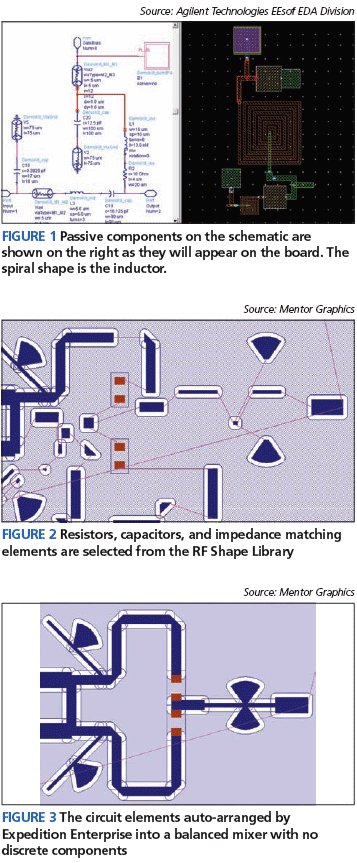
The software selects the appropriate discrete component shapes from the library, and also automatically assembles the shapes into a full RF circuit. In Figure 3, all component shapes have been selected from the library. The shapes are selected in an exact analog to assembling a PCB by picking the proper through-hole or chip component from the appropriate bin—but in this case, no components are mounted or purchased. These components are then automatically assembled in the final shape, in this case realizing a balanced mixer.
Importantly, this shape is now understood by Mentor’s Expedition Enterprise or Board Station XE as a fixed-parameter shape that must be moved intact. Within some limits, scaling is possible because the tools understand this is a circuit element, not just a collection of metal.
Additional RF parameters can also be defined, such as ground planes or keepout areas. Additional circuit elements can also be defined for requirements like meanders for impedance matching and stitch-vias for EMI and signal integrity. These are easily added with a semi-automatic process within the RF Solution.
The advantages of precise RF shape mapping
The advantages to printing precise components rather than assembling a traditional board using through-hole or chip components are many, especially in the RF domain where even tiny variances in component value or placement can cause a circuit to fail. The key is the maintenance of a robust library understood by both the PCB design circuit and the RF design and simulation tools.
- Part cost – The most obvious advantage in printing components is that it eliminates the cost of buying discrete components and lowers both inventory and assembly costs.
- Precision – When components are maintained in a library and printed on the PCB, the value tolerance can be much lower than for discretes. Greater precision on the PCB also means more precise simulations can be run.
- Crosstalk and coupling – Printing an entire circuit allows the PCB design software to maintain better component spacing and use ground planes and keepout areas to control the nasty effects of crosstalk and interstage coupling.
- Fewer iterations – When the layout and simulation tools understand each other’s environment and maintain joint libraries, simulation much more accurately represents how a circuit will perform on the actual PCB.
- Board usage – Printed RF components generally require less space than placed and routed discrete components. This leaves more space for the analog and digital circuits that reside on the same PCB.
- The bottom line – In addition to the direct savings associated with being able to print RF components, the other items in this list shave time off both design and layout. There are fewer iterations, less designer time, less test time, and the entire development cycle is shortened. In short, product cost is greatly reduced.
The ability of the PCB design software to now understand the relationship, maintain the parameters, and actively exchange data with the RF design and simulations tools, represents a massive leap forward in RF design in the presence of mixed signals. And, it trims a good deal of time from product design flows by eliminating re-spins just to tweak the RF circuitry.
Mark Forbes is content manager and technology writer for Mentor Graphics.