Military comms system requires new tools, flow and backplane
The contributor supplies high-end military communications systems to both the US and Canadian Navies and here describes the development of a new methodology and also a new backplane for a system that is now being retrofitted onto all ships in Canada’s fleet.
The project represented a tipping point. In specific terms, the changes were undertaken because the new target design involved too much density, too much data and too great a sensitivity to crosstalk and other EMI for the designers to continue to evolve the existing approach and technology.
However, the changes were also undertaken in the light of emerging technologies. For example, this design worked with 0.8mm-pitch BGA packages, but the company is now reviewing projects that will entail 0.4mm-pitch packages.
DRS is a military supplier, and our division, the Hardware Design Group, works on sophisticated communication systems, primarily for the Canadian Navy, the United States Navy, and a few other customers. Our products are very much at the high end and integrate both secure and non-secure voice communications as well as data. This article considers one of the most recent systems we designed as it entailed, among other changes, the introduction of both a new design methodology and a new backplane for the finished product.
The voice part of the comms system featured in the case study presents sound in three dimensions so that the user has an enhanced ability to comprehend multiple inputs. Technology this advanced, and the need to wrap it in a secure system, requires that potential noise sources such as crosstalk are virtually eliminated from every signal on the board. Secure and non-secure voice simply cannot bleed over into the other channel. This means the PCB design is very critical and requires intense simulation.
Before we designed this particular board, our design flow followed an essentially traditional path, although layout work was outsourced. By ‘traditional’, I mean that constraints were defined (to a point) and passed to the layout designer in a variety of inefficient ways such as a spreadsheet or a paper hardcopy. The designs went reasonably well, but our engineers and the layout designers would spend a lot of time on the phone.
However, an advance review of the new project showed that a new methodology was needed. It involved too much density, too much data and there was too much of a potential for crosstalk and other EMI for us to persist with an approach where the work of the hardware designers and the layout designers was almost completely decoupled. We needed something that we could take into the future.
New tools, new methodology
It quickly became clear that the new device would require some tools, planning, and layout savvy that we had never employed before. As mentioned, maintaining tight control over crosstalk and secure audio sections demanded a very careful layout. In addition, the boards entailed a volume of data that was significantly greater than we were used to. Ultimately, and as noted earlier, we needed to define a completely new backplane, replacing one that we had been using for about ten years.
The established backplane was VME-based and until then had been the de facto standard for military applications. But, at the data rates and volume required by this project, VME ran out of capability. Instead, we elected to design a complete new backplane using multi-gigabit Ethernet SERDES channels and a lot of DDR 2 memory to enhance the VME architecture. In addition to changing the backplane, incorporating all these functions at ramped up data rates meant we would have a very dense layout and would be using multiple 0.8mm-pitch BGA packages.
We consequently knew that we would have to use state-of-the-art tools to realize this design within the time and budget constraints. Adopting these tools meant that we also needed a new methodology and work flow.
We wanted to fully exploit a constraint management system. We also knew that there was no way to analyze signal integrity without simulation, so a simulation tool was needed. Our PCB layout design firm uses Mentor Graphics’ Expedition Enterprise, so our tools of choice were Mentor’s Constraint Editor System (CES) and its HyperLynx simulation tool, in addition to a tool with which we were familiar, DxDesigner.
Building the foundation
We knew that the use of netlists alone would insufficiently define the parameters, and that we could no longer tolerate any disconnect between design and PCB layout engineers. We found that entering constraints into the constraint manager initially appeared very time consuming, but having precise definitions and complete specifications ultimately saved many hours later on. The constraint manager made liaison with the layout designers much more efficient.
We defined the most critical nets first. Then, we moved to critical traces and the remaining nets. The layout designers said that their job became much easier when all parameters were explicitly defined at an early stage. As well as constraints, intent was communicated down the flow.
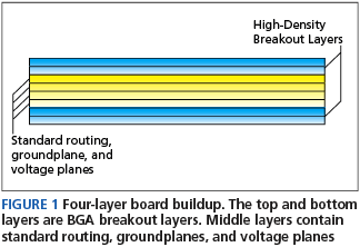
At about the same time, we began exploring board buildup. With the number of BGA packages and the fine pitch of the balls, we knew this would be a challenge. On previous products, we largely limited ourselves to standard through-hole vias. With this project, we elected to use vias-in-pad and microvias simply because we had no choice with all these BGAs to break out.
For board buildup—again, almost entirely because of the number of breakouts involved—we used two layers on the top and bottom that incorporated high-density microvias almost exclusively for the BGA breakouts. This was a new move for our company, but to accommodate BGA pitches at 0.8mm it was seen as laying necessary technological foundations for the future (indeed, we are now exploring designs with 0.4mm pitch). The breakout layers also helped us address signal integrity issues. Figure 1 illustrates the approach adopted.
Board layout and simulation
This board was far more complicated than anything we had done before, so, given also the new backplane, we were concerned about making our deadline. In fact, time previously spent in back-and-forth conversations with the layout provider was largely eliminated because constraints were far better defined. Consequently, we were able to stay on schedule and actually produced the new board in about the same time we had needed to produce earlier, less-sophisticated products.
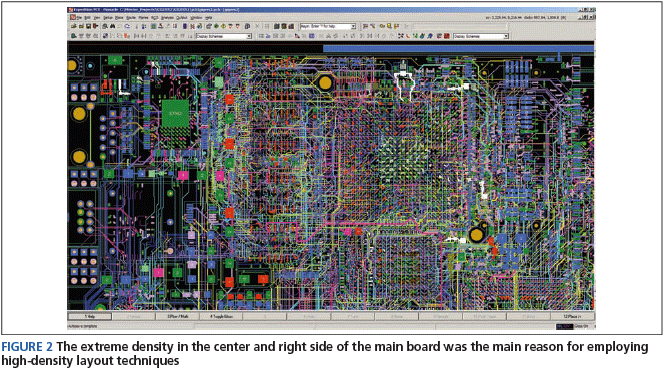
Figure 2 shows the layout of the main board. Clearly, this level of density places the utmost demands on both the designers and the design tools.
Simulation of the board, the new backplane and the interconnects followed layout, using HyperLynx. This process allowed us to make sure that the design met signal integrity goals. Incredibly, everything worked the first time.
Conclusion
This project had been an enormous challenge to all who were involved. Its scope was enormous; the constraints were many; the data rates and component densities were beyond what any of us had dealt with before. Yet, by employing the right tools, we exceeded our expectations. This was validated by the customer response, as they have already engaged us on another major contract based on this technology. Also, we are undertaking a complete redesign of our communications system based around the new backplane, and it will be retrofitted into systems operated by the Canadian Navy.
The biggest upcoming challenge is the rapidly increasing density of BGA packages—perhaps 0.4mm pitch in just a few years. This density requirement has made us realize that we simply cannot tackle this level of complexity without moving forward with PCB technologies such as microvias, HDI, blind vias, and breakout layers. All these factors will require better tools, better constraint definition, and better simulation. The tools have to keep up with packaging technology.
DRS Technologies Canada
115 Emily St.
Carleton Place
Ontario, K7C 4J5, Canada
T: +1 613 253 3020
W: http://www.drs.com