Inside the hot zone
 Floorplanning informed by thermal analysis can significantly improve PCB layouts, writes Robin Bornoff
The number of PCB design constraints seems ever increasing. The risk that a design will fail either functional performance or reliability goals grows for each generation. One increasingly popular trade-off addresses a balance between thermal compliance and signal integrity. Components with high clock speeds must be close together on the board to minimize signal degradation. But such components dissipate a lot of power and thus need to be as far away from one another as possible to reduce temperature.
This article considers a floorplanning strategy informed by thermal prediction and design optimization for an airborne PCB product. The PCB is wedgelocked to the inside of a chassis that has externally forced convection-cooled heatsink fins. Such harsh environments—with an aggressive local ambient air temperature and conduction as the main form of cooling—present serious challenges to achieving desired component junction temperatures.
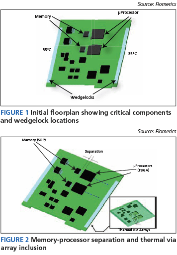
Figure 1 shows an initial floorplan. The external chassis provides a cooling temperature of 35ºC where the wedgelocks clamp to the PCB. The local air temperature is 75ºC. Although all components dissipate heat, microprocessors and memory components are the most thermally critical.
Design goals and constraints
There are many different ways of thermally managing a layout. In some way, all control how easily the heat dissipated by each component leaves to the available (cold) ambient temperature. In this example, the interaction between two ways that promote efficient heat removal is numerically predicted using Flotherm thermal prediction software.
First, the spatial separation between the memory and microprocessor components is varied, while that between the memory components is fixed. This moves the processors away from the thermal influence of the memory components and closer to the (cold) wedgelocked regions. Second, the software calculates the effect of including ever more densely populated arrays of thermal vias beneath both component types. Both techniques are shown in Figure 2.
The thermal vias allow heat to pass easily down to the internal metallic layers within the PCB, especially to the power and ground planes where it is easier for heat to conduct laterally to the cool wedgelocked sides. Without the vias, the heat faces more thermal resistance in its passage to the wedgelocks as it has to go through the copper coverage on the top signal layer.
Contemporary designs have signal frequencies measured in gigahertz and signal rise times measured in picoseconds. As such, the rise time is of the same order as the wavelength and the risk of critical signal deterioration is much increased. The separation between the memory and processor components therefore must be as short as possible—in this case, no more than 11mm.
The maximum rated junction temperature of the processors (packaged as a tape BGA) is 100ºC. Component suppliers provide some data that indicates thermal performance (e.g., the thermal resistance between the junction and the ambient temperature), but they are often only valid for a specific package deployment. For a design with many complex and competing thermal effects, the only reliably accurate thermal prediction is a 3D numerical simulation of the entire PCB assembly.
Thermal simulation
Simulation has traditionally focused on the study of a single set of parameters and then provided a ‘pass’ or ‘fail’ mark for verification. State-of-the-art numerical thermal simulations investigate the sensitivity of thermal performance to changes in the design. This approach lets designers more rapidly isolate the optimum combination of design parameters to reach the design goal.
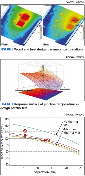
It begins with the creation of a ‘Design of Experiments’ (DoE). This is a collection of design variants constructed from combinations of those parameters that can be changed. In this instance, those parameters are the separation distance between the memory and processor components and the density of the thermal vias beneath those components. In all, 20 simulations are run to build up a picture of the full set of interactions between these parameters.
Figure 3 shows the two extremes of the DoE—the thermal performance when there are no thermal vias and the processor and memory components are close together, and the best combination where there is a dense array of thermal vias under all four components and the processor components are very close to the wedgelocks.
Response surface
The simulations provide some insight into the thermal behavior of the design. However, a more complete picture is achieved by fitting what is called a ‘response surface’ to the 20 data points. This response surface is, in effect, an advanced curve fit. It gives an overall representation of the complete interaction between design changes and the resulting thermal performance (Figure 4).
Note that the effect of thermal via density under the components is quantified as the resulting thermal conductivity down through the stackup. A value of 0.3W/mK (the thermal conductivity of FR4) is indicative of there being no thermal vias. A value of around 10W/mk indicates a highly dense array of thermal vias.
The response surface confirms one expected trend in the design: when the separation between memory and processor components increases, the maximum processor junction temperature decreases. However, the relationship between thermal via density and junction temperature is more interesting. Regardless of the separation distance, the difference on adding even a few thermal vias is marked. By comparison, further filling of the space under the components with thermal vias has a reduced benefit.
A more quantified observation can be made by taking various line ‘slices’ of Figure 4 at various thermal via array densities (Figure 5). The design constraints of component separation and maximum junction temperature are also indicated as ‘no-go’ areas in the plot. By looking at the response lines that reside within the allowed design space, it is evident that some thermal vias are required with a little margin to be had by maximizing the number of thermal vias under the components.
Conclusion
By performing numerical simulations during early floorplanning, performing a Design of Experiments, and generating a response surface, we can reach an in-depth understanding of a design’s response to various change scenarios. This in turn allows for a more rapid balancing of design trade-offs, while minimizing the risk that late design stage thermal problems will be introduced.
The example presented here considers the interaction of just two design variables. In fact, this simulation methodology can be applied to any number of interacting design parameters.
Robin Bornoff is product manager at Flomerics (www.flomerics.com).
