Board-level timing analysis
This paper builds on “Timing Numbers In ICX – What do we do with them?” [1]—a paper presented at the 2006 Mentor Graphics User2User conference (and now available for download at the journal’s Web site, www.edatechforum.com). The original paper focused on the need for timing analysis and the theory behind it; this paper takes a more practical approach. It examines two example circuits, showing when and how timing analysis is performed. The first is a conventionally clocked circuit. Since timing analysis is so different for source-synchronous interfaces, the second example addresses this area through analysis of a DDR SDRAM circuit.
This paper presents a methodology for board-level timing analysis, concentrating on two specific areas: pre-route (preliminary design) and post-route (PCB design). It shows how to perform the analysis and then verify the PCB trace delay portions using both HyperLynx and ICX. The aim is to demonstrate a practical way of performing board-level timing analysis for use on digital designs.
The background theory of timing analysis is not included here, and the paper assumes that the reader has a basic understanding of the procedure.
The need to simulate
Trace delay is a term in both setup and hold timing equations: a maximum trace delay is used in the setup equation; a minimum is used for the hold. The trace delays of clock routes in a conventionally clocked circuit must also be verified. And, in a source synchronous interface, the relative skew between different trace delays must be verified. We verify the timing of these signals with signal integrity simulation tools.
Pre- and post-route simulation
If we verify timing after we route the PCB, why verify it before routing has even started? Because pre-route simulation validates the design to the point where the likelihood of large, late-stage changes is significantly reduced. Sometimes timing just cannot be met without a large design change. It is far better to learn this during preliminary design than when you’re routing a PCB. The earlier simulation is performed, the smaller the impact a timing problem will have on schedules and budgets. The tool used here is HyperLynx.
Post-route simulation verifies that the PCB route details stay within rules established in the pre-route analysis. We will show how these trace delay rules are derived directly out of the timing analysis. ICX was the tool used for post-route analysis.
Example One
Any designer should be able to offer a general, conversational description of the timing of his/her circuits. In fact, write this description down—when you come back to this analysis a year or so later, you can ramp up the analysis very quickly by referring back to these notes.
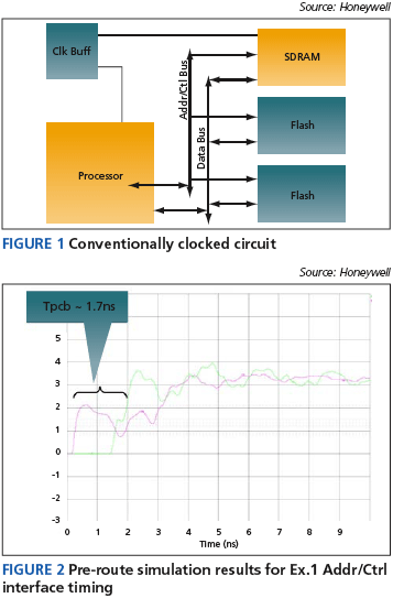
Example One is a conventionally clocked circuit. Figure 1 shows the block diagram. The timing analysis will be done on the ‘Processor’ to ‘SDRAM’ section. Wait states will be inserted for the ‘Flash’ so there is no timing issue in this section of the interface.
Timing analysis will cover setup and hold times of the 18bit ‘Addr/Ctrl’ bus, and the read and write phases of the 32bit ‘Data’ bus. The write phase has the Processor driving the data bus, the read has the SDRAM driving the data bus. The Processor always drives the Addr/Ctrl bus.
The design has a common clock sent to both devices. Clock skew will account for differences in the clock’s arrival time to either device and will always be subtracted in both the setup and hold equations. This subtraction of clock skew is always worst case.
Both the processor and the SDRAM are non-custom devices, so their timing comes directly from their datasheets (Tco (min & max), Thold, and Tsetup).
Timing analysis
The timing analysis contains three sets of setup and hold equations (Addr/Ctrl, Data Writes, and Data Reads) and the simulation results (pre-route and post-route).
The next step establishes the timing equation for each section of the interface.
Pre-route timing
Addr/Ctrl Setup timing:
SU(margin) =tCLK- tCO(MAX) – tPCB(MAX) – tCLKSKEW – tSU
0 =10ns – 5.5ns – ??? – 0.20ns – 1.5ns
If we allow margin to go to zero then:
tPCB(MAX) = 2.8ns
The 2.8ns here is the absolute maximum for PCB trace delay. As this is a pre-route analysis we should add some margin. We will start with a 2.0ns rule.
Addr/Ctrl Hold timing:
Hold(margin) = tCO(MIN) + tPCB(MIN) – tCLKSKEW – tHOLD
0 = 0.7ns + ?? – 0.20ns – 0.8ns
If we allow margin to go to zero then:
tPCB(MIN) = 0.3ns
Notice that trace delay for hold timing actually helps (it is added in the equation). The equation says that we need at least 300ps of trace delay.
Figure 2 shows that there is sufficient setup and hold time margin to confidently proceed into the PCB design phase using these timing rules.
The same approach is used for Data Write timing, except that it is on the data bus, and there is one less load (each data bit only goes to one of the Flash devices). It is also used for Data Read timing, except that, again, it is on the data bus, and there is one less load, although here the SDRAM is driving the bus.
Post-route timing
The trace delays established in our timing analysis and verified in the pre-route simulation now become the rules for our post-route simulation.
The actual maximum trace delays were substantially greater than the pre-route analysis anticipated (2.5ns instead of 1.8ns). This was caused by several factors: routing congestion, via parasitics, and topology compromises during placement. Much of the margin we started out with got used up in the actual route.
Example Two
This DDR SDRAM circuit contains a memory controller and SDRAM components. The controller is a custom-designed FPGA, so I/O timing rules established in this timing analysis will drive requirements for the FPGA designer.
DDR timing analysis review
The DDR method described in [1] will be used for this analysis. The equations used are shown here. Remember that even though this is a source synchronous interface there is still a setup and hold requirement for all flip-flops.
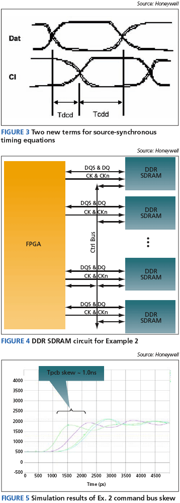
The terms ‘Tdcd’ and ‘Tcdd’ are defined in Figure 3.
Setup timing:
Setup Margin = Tdcd – Tdoskew – PCBskew – Trcvrskew – Tsu
Hold timing:
Hold Margin = Tcdd -Tdoskew -PCBskew -Trcvrskew – Th
Description of Example Two
Figure 4– shows the DDR SDRAM circuit. There is one bank of SDRAM that is 48bit wide—8 bits to each SDRAM device. The data bus is called the DQ bus. It is bi-directional and is a point-to-point interface (one driver, one receiver).
The address and control interface is called the command bus. The command bus is always driven by the FPGA. This is not a point-to-point interface. Most of the command bus goes to all six SRAM devices.
There are two clock domains in this circuit. The command bus is on the CK/CKn clock domain (125MHz). This is a single data rate interface. The command bus is clocked into the DDR SDRAM only on the rising edge of CK.
The data bus is on the DQS clock domain. The data bus (DQ(48..0)) is clocked in on both the rising and falling edge of DQS (a data rate of 250MHz). This is a bi-directional bus. During a data-write operation, the FPGA drives both the data bus and DQS. During a data-read operation, the SDRAM drives both the data bus and DQS. There are six DQS clocks: one to/from each SDRAM, and for each byte lane. There are three different transactions in this timing analysis: command bus, data read, and data write.
Command bus timing
Timing here relies on the FPGA to drive the command bus on the falling edge of CK. The SDRAMs will clock this information in on the rising edge of CK. This will allow Tdcd and Tcdd to both be 4ns. (NB: there are six CK and six CKn lines, one pair routed to each SDRAM.)
The setup and hold time equations are:
Setup Margin = Tdcd – Tdoskew – PCBskew – Trcvrskew – Tsu
0.5ns = 4ns – 1ns – 1.5ns – na – 1ns
Hold Margin = Tcdd – Tdoskew – PCBskew – Trcvrskew – Thold
0.5ns = 4ns – 1 – 1.5ns – na – 1ns
The margin is 500ps if the command bus PCB skew can be kept below 1.5ns. This does not seem too challenging until one realizes that the command bus must go to six SDRAM devices.
Pre-route simulation now becomes valuable. It approximates the distance and placement of the circuit and evaluates the settling time. The results of the simulation are shown in Figure 5, and indicate that the bus settles in less than 1ns. Therefore, the 1.5ns settling time relative to the CK route will be the rule used.
Data write timing
The data write timing centers around the FPGA driving the DQ(47..0) bus and the six DQS clock lines.
The timing equations are:
Setup Margin = Tdcd – Tdoskew – PCBskew – Trcvrskew – Tsu
0.5ns = 2ns – 0.5ns – 0.5ns – na – 0.5ns
Hold Margin = Tcdd – Tdoskew – PCBskew – Trcvrskew – Thold
0.5ns = 2ns – 0.5ns – 0.5ns – na – 0.5ns
Note that the PCB skew is much smaller than the command bus: 500ps. Also, there is no need for any pre-route simulation for timing of this bus (both read and write cycles). The reason is that the only thing that is needed is to match a routing skew of 500ps between all nets.
Data read timing
The data read timing centers around the six SDRAM devices driving the DQ(47..0) bus and the six DQS clock lines.
The timing equations are:
Setup Margin = Tdcd – Tdoskew – PCBskew – Trcvrskew – Tsu
0.25ns = 2ns – 0.5ns – 0.5ns – 0.25ns – 0.5ns
Hold Margin = Tcdd – Tdoskew – PCBskew – Trcvrskew – Thold
0.75ns = 2ns – 0ns – 0.5ns – 0.25ns – 0.5ns
Conclusions
This paper described a method for performing board-level timing analysis. It attempted to establish the importance of performing this analysis (along with the theoretical fundamentals) and also proposed a methodology. Using this paper and presentation as a guide, you should be able to successfully perform timing analysis on your next board design.
Reference
- “Timing Numbers In ICX – What do we do with them?” User2User 2006, available online at www.edatechforum.com.
Honeywell Space Systems
M/S 934-5
13350 U.S. Hwy 19 N.
Clearwater
FL 33764-7290
USA
www.honeywell.com