Switch to orbit mode boosts MRAM on 300mm wafers
Imec will at this week’s VLSI Symposia describe how it fabricated a form of magnetic memory suitable for use as a non-volatile cache onto 300mm wafers using CMOS-compatible processes.
The research institute’s team opted to use the spin-orbit torque (SOT) form of MRAM. Offering a switching time of 210ps and power consumption of 300pJ, Imec said when manufactured in a 300mm line the SOT-MRAM devices achieve the same or better performance as lab devices.
The mechanism used in SOT-MRAM devices was first demonstrated by researchers at the Catalan Institute of Nanotechnology in 2011. Proponents argue it offers lower-power switching and much higher endurance than the spin-torque transfer (STT) technique used in the latest generation of commercial MRAMs because it demands much lower current levels. The SOT-MRAM takes advantage of a property of the symmetry of certain types of crystal that lead to a momentum-dependent difference in band energies for electron spin states.
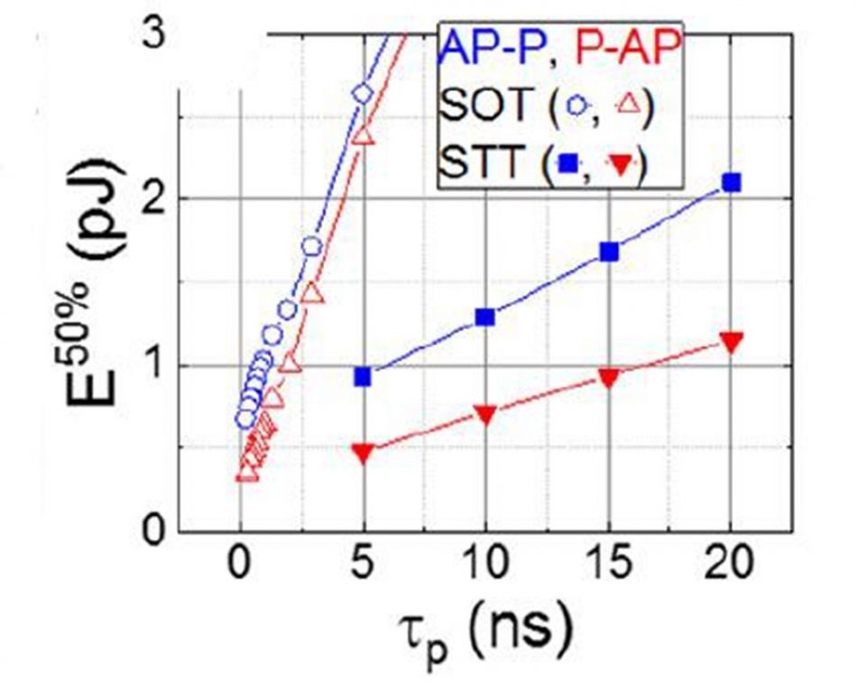
Image Energy comparison of SOT and STT switching for the Imec device
At the core of the SOT-MRAM device is a magnetic tunnel junction in which a thin dielectric layer is sandwiched between a magnetic fixed layer and a magnetic free layer. Similar as for STT-MRAM operation, writing of the memory is performed by switching the magnetization of this free magnetic layer, by means of a current. In STT-MRAM, this current is injected perpendicularly into the magnetic tunnel junction, and the read and write operation is performed through the same path – challenging the reliability of the device. In an SOT-MRAM device, on the contrary, switching of the free magnetic layer is done by injecting an in-plane current in an adjacent SOT layer – typically made of a heavy metal. Because of the current injection geometry, the read and write path are de-coupled, significantly improving the device endurance and read stability.
Imec argues its approach to manufacturing can take the SOT-MRAM out of the lab and into production. The researchers claim the memory would be fast enough to support level-one and level-two cache requirements and also offering non-volatility.
In its experiments, Imec compared SOT and STT switching behavior on the same device fabricated on 300mm wafers. Whereas switching speed during STT-MRAM operation was limited to 5ns, reliable switching down to 210ps was demonstrated during SOT-MRAM operation. Tests indicated SOT-MRAM operation would let the device endure more than 5×10¹⁰ switches.
In these devices, the magnetic tunnel junction consists of a SOT/CoFeB/MgO/CoFeB/SAF perpendicularly magnetized stack, using beta-phase tungsten (W) for the SOT layer.
“STT-MRAM technology has a high potential to replace L3 cache memory in high-performance computing applications”, says Gouri Sankar Kar, distinguished member of technical staff at Imec. “However, due to the challenging reliability and increased energy at sub-nanosecond switching speeds, they are unsuitable to replace the faster L1/L2 SRAM cache memories. SOT-MRAM technology will help us to expand MRAM operation into the SRAM application domain. By moving this next-generation MRAM technology out of the lab, we have now demonstrated the maturity of the technology.”
Future work will focus on further reducing the energy consumption, by bringing down current density and by demonstrating field-free switching operation.