Watch out for layout effects on finFET reliability
As geometries have shrunk, layout-dependent effects in CMOS have become ever more problematic. They are not just popping up in performance but reliability and aging effects, as researchers from the Key Laboratory of Microelectronics Devices and Circuits in Beijing, described at the recent IEDM conference in an invited paper.
The team described (“Variability- and Reliability-Aware Design for 16/14nm and Beyond Technology”, Huang et al) a number of studies into the performance and reliability problems faced by the finFET-based processes, from which they have derived modeling techniques.
In terms of performance, the main random sources of variation in finFETs continue to be around the granularity of crystals in metal gates and line-edge roughness. This is not helped by the continuing extension of optical lithography. Such effects are found also in planar technologies. However, a problem identified by the Beijing researchers is a rising negative correlation between subthreshold swing and threshold voltage can lead to the effects being either over- or underestimated by traditional models, which has implications for near-threshold design.
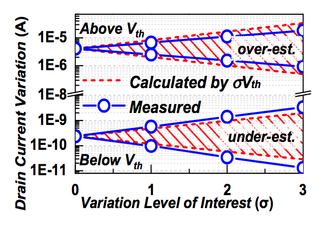
Image Over- and underestimation of variation in devices based on Vth analysis without subthreshold swing prediction
Above the threshold voltage, variation could easily be overestimated but underestimated for substhreshold operation. Adding consideration of subthreshold swing to the model versus a simpler technique that takes into account just threshold voltage not only shifted to the right the probability distribution of static noise margin in SRAMs but tightened it. To take account of these effects, the Beijing team proposes a design methodology that uses statistical matching to help with the selection of appropriate gate dimensions for finFET transistors used in near-threshold circuits.
When it comes to reliability, effects such as bias temperature instability (BTI) continue to become more apparent. A key challenge is the way BTI can recover, which makes the prediction of aging effects difficult to accomplish. FinFETs do not make this easier. In contrast to planar devices, finFET appear to demonstrate a two-stage form of degradation and recovery. Traditional linear models tend to encourage overdesign.
However, finFETs are prone to layout-dependent BTI issues that were first uncovered in 28nm HKMG. Negative BTI tends to worsen with reducing source and drain lengths, which is not unexpected. But NBTI improves if the spacing between linked NMOS and PMOS gates is kept small. A paper by the group presented at IEDM in 2015 speculated this could be due, in HKMG proceses, to traps in PFETs being eliminated by the diffusion of nitrogen ions from the TiN gates of the NMOS devices.
As devices continue to scale, trap behavior is likely to become worse. The team proposes the use of enhanced prediction techniques to account for statistical BTI and other effects.