ISSCC 2013: AMD constraints help tame Jaguar
With its specification inside the PlayStation 4 and a spec debut at ISSCC, AMD is getting all the performance headlines it could wish for Jaguar, its first 28nm HKMG x86 core.
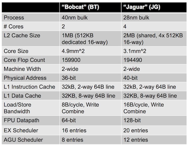
Designed to scale across a wide range of applications from sub-5W to 25W although interestingly a day before Sony’s announcement, the ISSCC slide deck only went as far as a “value desktop” – the core marks significant advances over its Bobcat predecessor. These are summarized in the table at the foot of the page. However, for Sony, the ability to get the clock up beyond 1.85GHz will have been important to its choice of a technology that will probably not reach such speeds in most implementations.
But what about some of the more interesting design decisions.
First, area was a major concern with Jaguar, yet AMD was able to build the core as a single block using standard place and route tools (a pat-on-the-back for EDA, but a pity they didn’t name the vendor).
“A high density nine-track library is used with an 11-metal process that has eight 1x metals to balance place and route utilization,” the company said. “All register file arrays are constructed using guides to force regular structures for reduced clock power and improved overall routing.”
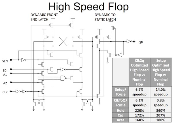
Then AMD played cautiously when it did come to a custom element: flip-flops specifically designed to deliver better performance. A dynamic front-end latch improves setup time, and the stacked front end itself addresses leakage and “enables simple integrated combinational logic and MUXD scan”. The custom flops also exist in variations that allow the clock path to be shortened and tradeoffs between setup and clock-to-q delay.
Figure 1. Jaguar high-speed flop with embedded MUXD scan and combinatorial logic (Source: AMD/ISSCC2013/IEEE).
However there is a ‘but’. “While providing significant performance advantages over AMD’s previous generation products, these larger flops consumer more dynamic power,” AMD said.
“To minimize the power and area impact, they are inserted only in critical paths. Automated tools are used to select the optimal variant depending on critical timing.”
In all, the custom flops make up less than 8% of all those in the core.
Then AMD also cut back on the number of memory modules from eight in Bobcat to just two in Jaguar, a RAM and a ROM. Two factors influenced this decision: cutting the timing closure iterations and making for easier process porting (Jaguar is manufactured on TSMC’s 28nm HKMG process).
Going into more detail, AMD disclosed the following about the RAM module.
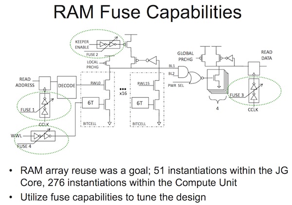
“The RAM module is a 2KB array with reundancy and is used in 32KB instruction cache. A slight modification is supported so that the same macro can be used for the data cache. The highly utilized RAM macro is instantiated 51 times in each core and 72 times in the L2 interface. The RAM macros have fuse-controlled tunable clock delays which can be adjusted independently for macro input and output delay. These clock delays allow for easier silicon debug and frequency adjustment,” the AMD paper says.
“This macro also includes an adjustable write-chop circuit which allows for silicon write-margin testing.”
Figure 2. RAM fuse capabilities (Source: AMD/ISSCC2013/IEEE)
There is a lot of cool stuff in Jaguar, but the Processors session at ISSCC has over the years become more about playing up bragging rights than acknowledging design constraints and innovation through off-the-shelf technologies and methodologies. So, it was nice to see AMD acknowledge the ‘other side’ – though such kudos probably isn’t as important to the Jaguar team as the kick-off Sony design win.
Meanwhile, here’s the traditional comparison.
Figure 3. Core comparison (Source: AMD/ISSCC2013/IEEE)


