ISSCC 2013: IBM adds digital logic synthesis methodology for System z
IBM’s 32nm HKMG System z MCM is chunky, as you might expect. It’s made up of six six-core 5.5Ghz CPUs and two 192MB L4 cache chips. The earlier 5.2GHz 45nm generation had four cores and L4 was half the size. Overall, the new MCM offers a 25% improvement on per-thread performance for traditional mainframe applications against the previous generation.
In its ISSCC presentation, IBM disclosed some of the design decision made with particular regard to the core and external (‘nest’) logic, and also how it addressed concerns over different bias temperature instability effects inherent in the use of high-k, metal gate at the new node.
For digital logic, both core and nest, it needed to implement a new methodology: Large Block Structured Synthesis. The higher frequency target was also an influence here. Beyond that, IBM also discussed BTI with particular reference to pulsed-clock latches used extensively across the design.
“This methodology incorporated novel algorithms to create structure in dataflow regions within the context of larger synthesized blocks,” said presenter James Warnock, a distinguished engineer within the company’s Systems & Technology Group.
“The success of this new approach led to a fundamental shift in the digital logic microprocessor design methodology from highly custom-oriented transistor-level designto a highly productive automated gate-level, synthesis-based LBSS.”
The theme of looking for still further automation even on bleeding edge projects recurred during ISSCC’s processor session with AMD’s description of its new low-power, general purpose Jaguar processor.
The results of a structured synthesis implementation are shown in Figure 1.
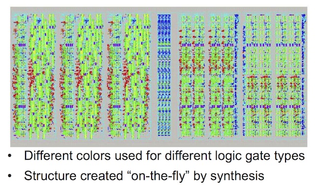
Figure 1. Design implemented via structured synthesis. Different gate types are indicated with different shading tones to highlight the detailed structure. (Source: IBM/ISSCC2013/IEEE)
For BTI, both negative (NBTI) and positive (PBTI), IBM’s focus fell on how clock pulse-widths and latch transmission gates were affected by prolonged voltage stress.
An in-house tool was used to apply waveforms transistor-by-transistor, with the results matched against a BTI model. It found that write margins increased over time, a fact confirmed by statistical analysis of the derived end-of-life parameter shifts. These results are illustrated in Figure 2.
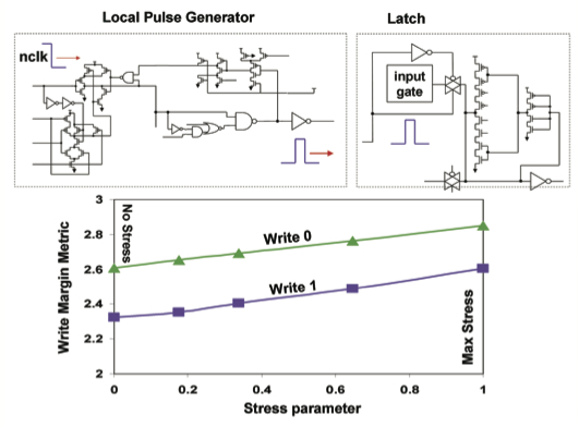 Figure 2. Pulsed-latch write-margin metric as a function of device stress. The “stress parameter” is a relative measure of the device level stress-induced VTH shift. (Source: IBM/ISSCC2013/IEEE)
“[This] was determined to be a result of the fact that the critical transmission gate devices receive relatively little stress (only when the pulsed-clock is fully active), while devices in the pulse generators see a more uniform level of stress,” Warnock said.