Degrees of freedom for finFETs
The crossover between design and process technology is more apparent than ever at the VLSI Symposia this week in Honolulu, Hawaii.
The first session of the short course that precedes the start of the technology program underlined the close interrelationship between design and process for the application of finFET and trigate transistor structures as their use permeates from Intel across the industry, and it’s a subject that continues through the day.
From one perspective, even ultra-thin body (UTB) or fully depleted (FD) silicon-on-insulator (SOI) can be viewed as part of a continuum of design that attacks the biggest source of performance degradation for low-power devices: drain-induced barrier lowering (DIBL). In her tutorial session, one of the key developers of the finFET at the University of California at Berkeley Professor Tsu-Jae King Liu described the tradeoffs that are possible between different variants of transistor structure, from tall, thin fins to very flat FD-SOI devices, as well as the use of doping in structures that, historically, have been considered to be mostly undoped.
King Liu explained that the genesis of the finFET began with the publication of a seminal paper by Digh Hisamoto of Hitachi Central Research Labs in 1991 that described the use of a tall, thin raised channel. This crystallized at UC Berkeley, where Hisamoto was a visiting fellow, when Professor Chenming Hu and his team put together a project to respond to a 1997 call from DARPA for a transistor structure that could scale down to 25nm.
By the early 2000s, the lab had demonstrated an architecture that scaled down to 15nm. “Then we collaborated with AMD and transferred technology into their fab to demonstrate the first 10nm finFETs. This proved that the double-gate finFET could take us to 20nm and beyond,” King Liu recalled. “Then Intel came up with the trigate FET fabbed on SOI. It is wider than it is tall, that’s why it is called trigate – there is a lot of current flowing along the top wall. It can’t be very tall,” said King Liu, as the gate begins to lose control of the carriers that flow along the base of the channel.
If you make the ‘fin’ very flat and wide, you effectively wind up with an FD-SOI, although it is not a double-gate device in the way that a finFET is. You can alter the fin height and width for a given doping profile for constant DIBL along an L-shaped curve – a tradeoff that Intel’s Ji-Woon Yang and Jerry Fossum identified in their 2005 paper.
Xin Sun and colleagues at UC Berkeley extended the analysis to include doping in a paper published in IEEE Electron Device Letters in 2008. It turned out in that analysis that the doped bulk version had better DIBL control than an equivalent SOI-based trigate structure. This makes it possible to increase both the fin width and height and keep DIBL constant. This process has already happened in the shift towards the use of bulk rather than SOI wafers for the substrate. To prevent current leaking into the bulk wafer, a steep doping profile is needed to ‘lock’ the carriers into the channel.
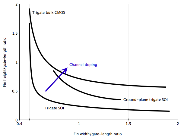
Graph showing fin width/height scaling for constant DIBL (simplified from Sun et al, EDL 2008)
“For circuit designers there are some considerations” when it comes to scaling height and width, said King Liu. “The taller the fin, the more current it can handle. But it becomes more difficult to manufacture.”
Width is another dimension that cannot go too far in one direction. “If you want to scale below 10nm, it turns out that the source and drain gradients can be significant sources of random dopant fluctuations. If the fin width is too narrow, then variation in off-state current becomes significant. You can’t scale fin width below 1.5nm because of this variation,” said King Liu. “So we need to relax the fin width requirement. The only way to do that is to shorten the fin. It turns that if you have doping at bottom, the shorter the fin the more helpful that doping becomes.
“So the trigate becomes shorter and wider. If you can extend the gate below the channel, that helps. So we might see some gate all-around devices in the future. As we scale below 10nm I think we will have gate all-around devices.”
Tomorrow’s session will show how doping could address another issue of finFET design: threshold voltage control. But there will be drawbacks: variability because of the dopants will increase compared with undoped channels and the fin-based devices could experience floating-body effects that will cause additional headaches for designers. Doping will also control how tight the fin pitch can get – tighter fin pitch will help density, particularly as fins tend to come in twos because of the self-aligned manufacturing techniques they require, but tight fins cause problems for doping control. How companies deal with those tradeoffs will require close interaction between process technologists and designers.