Bringing fabless players into manufacturing research
Sematech, the leading research consortium for semiconductor manufacturing, has launched a campaign to recruit members from the fabless sector. The move reflects the importance of making manufacturing decisions earlier in the design flow, and is also intended to get input from designers on implementations of such technologies as 3D interconnects, next-generation lithography and novel materials/structures.
This June, Sematech, the international manufacturing research consortium, welcomed on board an ‘unusual’ member.
Qualcomm is a massive player in the communications semiconductor business, but it is also a fabless company, outsourcing all production of its chips to foundries. As such, it was Sematech’s first fully fabless member of such scale, and the first to join under an active recruitment scheme that the consortium’s president and CEO, Dan Armbrust, had launched earlier in 2010.
The thinking behind the call to the fabless companies is simple. The assumption that chip manufacturing presents so many new challenges at each node that no one company can ‘go it alone’ does not extend solely to traditional back-end players, typically IDMs, foundries and packaging/test suppliers.
It is already accepted that EDA will play an increasing role here—as demonstrated by the surging market for design-for-manufacturing tools—but growing complexity also requires input from and an understanding on the part of those companies that may internally concentrate on chip design alone. They are now 20% of the industry, for one thing (Figure 1, p. 42).
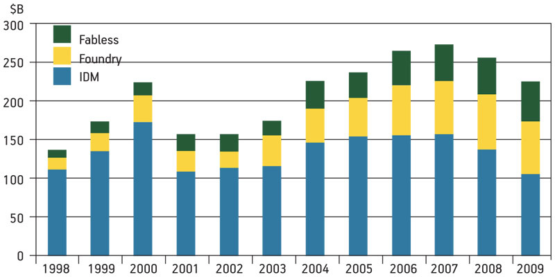
Figure 1
Chip production values by sector
Sematech’s contention is that the more of the supply chain it incorporates, the better placed it will be to deliver the manufacturing innovations that enable that broader goal.
Objectives
In a presentation to September’s Sematech Symposium in Japan, Ambrust set out five overarching trends that underpin his organization’s desire to recruit more widely.
- A declining growth rate for semiconductor revenues.
- Increasing technical and financial challenges to meeting milestones on the ITRS roadmap.
- Consolidation among manufacturers and suppliers.
- Evolving business models leading to greater industry segmentation and diverging technology differentiation.
- The increasing acceptance of a need for collaboration to meet emerging challenges.
He argued in turn that this quintet produces a quartet of consequences.
- There will be further consolidation down to just three or four main platforms, while remaining players take on increasingly specialized roles.
- Technological leadership will be defined by more than simply the ability to enable or achieve classical scaling.
- Research and development (R&D) costs will continue to escalate.
- Greater emphasis on collaborative R&D frameworks for the coordination of effort and innovation will be necessary.
To review the power of his argument, let’s consider what are arguably the three of the most pressing fields that raise those challenges: 3D interconnects, lithography and device structures (Figure 2).
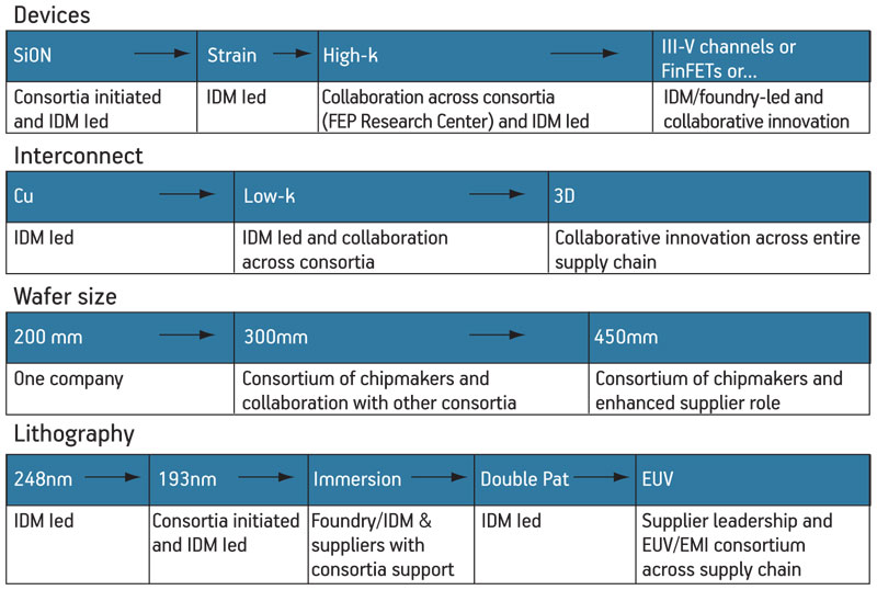
Figure 2
Leading manufacturing challenges
3D interconnects
The use of 3D interconnects is viewed in many circles as potentially both a very cost-effective and very pragmatic way of continuing to meet the economic and performance goals enshrined within in Moore’s Law.
“The technology is potentially worth a generation of scaling without scaling is one way of looking at it,” says Ambrust.
By allowing for a number of layers with high-performance links, 3D would also appear to enable the heterogeneous integration of various system elements that sometimes refuse to sit together comfortably or conveniently on a single piece of silicon. System-on-chip without the tears (well, some of them, at least).
However at a very basic level, 3D is still subject to a diversity of options. Should a design take a ‘via last’ approach that requires wafer-to-wafer bonding, or a ‘via mid’ approach with die-to-wafer bonding?
Such divergence can persist as devices move into volume production—or that has been the case today. Ambrust’s presentation in Japan cited two sets of obstacles to deployment in particular.
In the first, he noted that an immaturity in the tool infrastructure and even the materials could be seen. “There are numerous technology options and process flows. Several key tools have extremely low productivity, and cost-effective solutions are required for high volume manufacturing,” Ambrust said.
In the second—closely allied to the first—Ambrust identified “gaps in the supply chain.” He said that the especially pressing issues here were the “partitioning of new processes” within that chain, and the lack of standards that will ensure that chips from different vendors can be combined together with some guarantees of success in the same 3D system.
Sematech has itself begun to run workshops specifically aimed at promoting an alignment of this 3D supply chain. Two have already taken place this year at Semicon events in the U.S. and Taiwan.
The overview Sematech offers for core participants in this supply chain sets out a central role for fabless companies (Figure 3, p. 44). And that is hardly surprising given that the cost-effectiveness of 3D and related stacking and system-in-package techniques are seen as having an innate attraction to companies working on tighter, start-up type budgets.
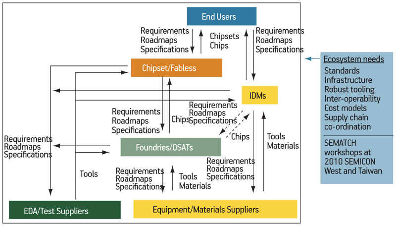
Figure 3
Building a 3D infrastructure
Lithography
Sematech remains strongly convinced that the industry will transition to extreme ultraviolet (EUV) lithography at around 13.5nm, some time before 2015. To that end, the consortium argues that a number of infrastructure enablers are already in place and several metrics have been met. Foremost among these are power sources, resist resolution, reticle protection and optics quality.
It is therefore concentrating on a fifth area—defect-free masks. This work is being directed through Sematech’s EUV EMI (mask infrastructure) program. This is the project that Qualcomm joined earlier this year.
So what has made Qualcomm’s jump? In Ambrust’s view, their decision is a vindication of the view that there is a process now taking place where these companies are so large that they should try to fund it, influence it and monitor it.
“What you see with Qualcomm is an understanding from them that, as a company that has taken an aggressive view on putting its devices on advanced silicon, it wants to know what is going on here and what implications it might have for its business.”
Ambrust acknowledges that EUV is not entirely a settled issue. There are competing claims for immersion and computational lithography strategies. His view is that the winning technology will be that which can assemble the right depth of infrastructure at the right time and claim the support of a critical mass of market players at a time when the number of those with influence is shrinking.
Device structures
Nanowires, FinFETS, NEMS. Graphene, III-Vs and chaclogenides. Not only future devices structures but also the materials they will use present a potentially confusing array of options to the market. As noted earlier, such diversity can lead to confusion, can stifle infrastructure development and delay innovation.
Here, current Sematech thinking does have IDMs and foundries leading the way, along with their academic counterparts. A certain closeness to process execution and materials science resides naturally in those companies. However, it is again, something that every company needs to track.
“Also, I think that we start to really see the importance of system-level thinking here, and that’s the big change that’s sitting underneath all these specific technological challenges,” says Ambrust. “You look at these things and you see the potential for their impact across the supply chain.”
To that extent, device structures are also areas in which all design engineers have a role to play. IDMs may have more ‘natural’ experience, but at those conferences that really attack this area—such as this month’s IEDM in San Francisco—contributions can also come from the fabless sector.
Conclusion
The basic ideas behind Sematech’s pitch to the fabless community lie, in their essence, within Ambrust’s comments in the section immediately above.
Since 90nm, the increasing importance of design-for-manufacture has alerted every participant in chip design to the need to push fabrication up the flow. That pressure is not going to reduce. However, alongside Ambrust’s manufacturing-centric view of the increasing role for system-level thinking, consider how easily it dovetails with such traditional ESL concepts as virtual prototyping, design space exploration and ‘what if’ scenarios.
For now, Sematech is looking to establish dialogue with the biggest players in the fabless sector. That is no surprise. Companies like Qualcomm have the resources to participate as equals in cutting-edge research with IDMs, foundries and equipment manufacturers. But the work under way has wider implications—and these will become apparent in a relatively short period of time. There is something here that requires monitoring, at least, by all.
Sematech
2706 Montopolis Drive
Austin
TX 78741
USA
T: 1 512 356 3500
W: www.sematech.org
