Hierarchical signoff of SoC designs at advanced process nodes
Hierarchical signoff strategies for large SoCs at advanced nodes can be effective if sufficient attention is paid to reflecting the impact of cross-hierarchy parasitics.
Advanced node SoCs integrate hundreds of functional blocks to achieve the rich features required from today’s electronics. As these designs grow to hundreds of millions of instances and their product cycle times shrink, design teams look to smarter divide-and-conquer methodologies to efficiently partition, extract, and verify their chip timing.
One approach to achieving this is to use hierarchical methodologies, which are becoming increasingly popular as the volume of data, the complexity of analysis, and the time required to verify advanced SoCs grows.
Designing at advanced nodes makes it more difficult to maintain accuracy in a hierarchical extraction and sign-off flow, because extra care must be taken to manage cross-hierarchy parasitics and to account for process-related variation. These factors affect parasitics and timing at both the block and top levels. Understanding the sources of potential inaccuracies and how to mitigate their effects enables design teams to develop robust hierarchical design methodologies, to improve the efficiency of the signoff extraction and timing closure phases of the design flow.
The flat approach to extraction and timing analysis
In traditional design flows, final extraction and static timing analysis (STA) are done ‘flat,’ extracting parasitics of the entire design down to the standard-cell level and exposing the complete layout environment for analysis. This ensures that any timing analysis carried out within a large functional block also takes into account any impact from top-level or adjacent-block routing parasitic effects, as in Figure 1. Flat signoff therefore provides very high accuracy, but when designs grow to 100 million instances or more, this approach can result in long runtimes and require many high-capacity computing resources.
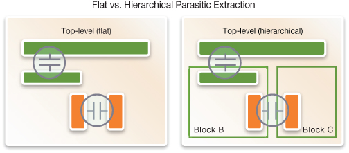
Figure 1 Hierarchical extraction needs attention to interactions between levels (Synopsys)
The hierarchical alternative
In a hierarchical methodology, the design is first partitioned into manageable blocks or sub-chips, based primarily on functionality. The objective is to make it possible to verify and close the timing for each of these smaller blocks in isolation, for faster individual turn-around time and thus faster timing closure for the overall SoC design cycle.
Once each block has achieved timing closure, it is integrated into the top level of the design, where special care must be taken to prevent the top-level placement and routing from interacting with the parasitics and timing of the blocks. This is particularly important at advanced nodes, due to the pronounced impact of shrinking geometries and the growing influence of process variation on resistance and capacitance values. The following sections identify some key sources of parasitic interaction between the top level of a design and the blocks within it, and outline some techniques to reduce their effects.
Dealing with cross-hierarchy parasitics in a hierarchical flow
It is important to reduce or prevent capacitive coupling effects between nets on different levels of the design hierarchy (e.g. from the top level to the block level) or between nets inside blocks at the same level. At advanced nodes, these effects are pronounced due to finer metal pitches and more stringent metal-fill density requirements. When placing a block, designers must consider the top-level routing environment and its capacitive effects on the block boundary nets, such as capacitive coupling from parallel routes on the same layer, and/or from routes that cross the block on higher metal layers.
One way to reduce these effects at block boundaries is to use correct-by-construction layout rules that limit how closely the top-level routing can approach the block-level routing. For example, designers can create a routing blockage, or ‘dead zone’, which defines a distance or number of tracks from the block boundary within which top-level nets cannot be placed. Similarly, designers can eliminate interactions with over-the-block routes by defining route blockages on top of the block and limiting top-level routing to areas outside the block boundary.
Another approach to top-level design is to abut the blocks, so that they need almost no top-level routing other than a mesh network for power, ground, and clock signals. This makes the block placement environment very predictable. Block and top-level routing are clearly separated and restricted to specific metal layers, for example by limiting block-level routes to layers up to metal 8, and allowing metal layers 9 and above to be reserved for top-level routes or redistribution layers (RDL). Since there is no routing area between the blocks, top-level routing must run over the blocks, which means its impact on block-level timing must be accounted for. Designers can predict the timing impact of this routing at the block level by placing a mesh overlay on the higher metal layers of the block during timing analysis, to mimic the clock or power/ground mesh that will exist in the top-level design environment. This is shown in Figure 2.
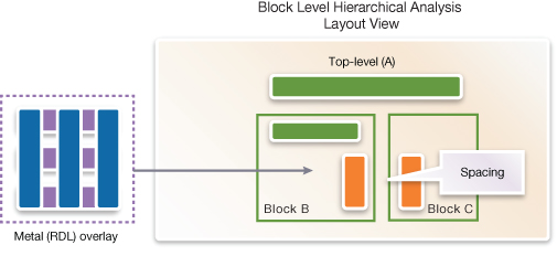
Figure 2 Block-level extraction needs accurate modeling of environmental effects (Source: Synopsys)
The impact of process variation in a hierarchical flow
Another important aspect of hierarchical design at advanced nodes is predicting the impact of silicon process variation on parasitics and timing when blocks are placed in the top-level environment. Local variations in capacitance and resistance, stemming from sub-16nm process effects such as multi-patterning lithography, are influenced by both the width and spacing of adjacent conductors.
Designers can control the spacing and width of top-level nets adjacent to their timing-closed blocks, enforce wider spacing rules, or route blockages between block boundaries and top-level routing. Another approach to model the local process variation at the block level is to introduce a shield ring around the block to mimic an aggressor net and therefore account for the worst-case scenario in the block’s timing closure.
It is also important to anticipate the global impact of the chemical-mechanical polishing (CMP) process on block resistance and capacitance at advanced nodes. Block designers must be able to model and predict the metal density of the environment after the blocks are placed. The actual impact of CMP on nets routed close to a block’s boundaries depends on the metal density gradient in a relatively large area outside of the block, as shown in Figure 3.
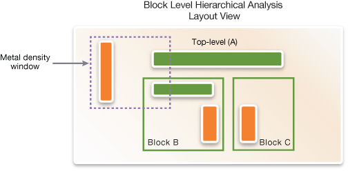
Figure 3 Block-level extraction needs accurate modeling of metal density variations (Synopsys)
The thickness of the conductors on the block boundary might vary significantly. The change in conductor thickness affects the capacitance of the net, and has two effects on its resistance. The first is that as the wire’s thickness and cross-sectional area decrease, its resistance increases. The second is that the resistivity (rho) of the copper wiring increases because of the effect of ion scattering, due to changing physical properties. Due to this density-dependent impact on parasitics, designers must predict the possible metal pattern-density gradients that will exist around the block once it is placed, in order to extract parasitics and close the block-level timing.
The importance of having the right level of detail
Designers at the top level must also deal with the effect of process variation after integrating hierarchical blocks. Figure 4 shows that blocks placed hierarchically can be represented at the top level using a variety of abstract views for parasitic extraction, including the open standards DEF (Design Exchange Format), GDSII, and LEF (Library Exchange Format).
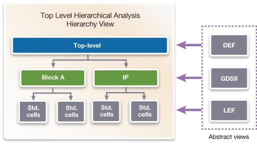
Figure 4 Top-level hierarchical analysis needs detailed abstract views for accurate signoff (Synopsys)
For top-level parasitic extraction, detailed GDSII or DEF representations of the hierarchical block must be provided to accurately account for metal density-related process variation on boundary nets. This information must be provided alongside the simplified abstract views, such as LEF data, that were sufficient at older process nodes. Similarly, for densely placed standard cells, the detailed GDSII files for the full library should be provided during parasitic extraction to accurately account for CMP-related process variations. If the proper views are provided for top-level analysis, designers can accurately model the impact of process variation.
Conclusion
Hierarchical design and signoff for advanced node designs are useful alternatives to the more time-consuming and resource-intensive flat design methodology, enabling designers to use divide-and-conquer techniques to break up complex design and analysis problems into more manageable pieces. However, using hierarchical sign-off at advanced nodes requires care to properly handle across the design hierarchy both the parasitic effects from close-proximity nets and any global process variations. A hierarchical flow that manages such issues effectively can improve productivity and match the signoff accuracy of a flat flow.
Author
Omar Shah is a principal applications consultant at Synopsys. He has more than 15 years of professional experience in the semiconductor and EDA industries working on post-layout digital and custom design flows. Shah holds MSEE and BSEE degrees from California State and Purdue University.
